PCB Fiducials: Size, Placement, and When You Need Them
PCB fiducials are optical reference marks that enable accurate board alignment and component placement during automated assembly. Their design depends on alignment requirements, board layout, and equipment capabilities. Key considerations include fiducial quantity, size, spacing, solder mask openings, and optical clearance.
Get Your PCB Quote!

Table of Contents
Table of Contents
PCB fiducials are optical reference marks that help automated assembly equipment locate a board, panel, or critical component area. A camera finds the known marks, compares their measured positions with the design coordinates, and corrects placement for X-Y offset and rotation. A third non-collinear mark can provide an additional reference for scale or skew checks when the machine’s alignment model supports them.
The right layout depends on what the machine must align. Panel fiducials locate the production panel, board or global fiducials locate an individual PCB, and local fiducials refine alignment near a component. Terminology varies: some manufacturers use “global fiducials” to include panel-level marks. This article separates panel and board/global marks because they align different physical references. Treating all three as one interchangeable set is the source of many quantity and placement mistakes.
What Are PCB Fiducials and How Do They Work?
A PCB fiducial is usually a solid circular copper target with no solder mask over it and a clear area around it. It is created with the circuit artwork, which gives the vision system a repeatable feature tied to the PCB coordinate system.
During setup, the machine moves its camera to the expected fiducial locations. The measured centers show how the physical board differs from the programmed coordinates. With two separated marks, the machine can correct X and Y displacement and board rotation. A third non-collinear mark provides another reference that some machine alignment models use to check scale or skew. It does not mean that three marks can compensate for arbitrary board warpage or distortion.
A fiducial is different from a tooling hole, mounting hole, test point, or silkscreen dot. Those features may be visible, but their geometry, finish, or positional tolerance may not provide a stable optical center. A dedicated fiducial gives the assembly program a known target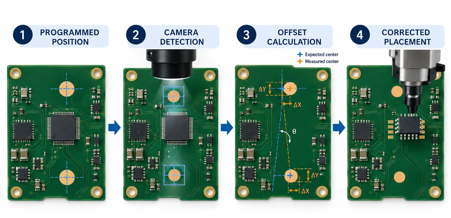
When Do You Need Fiducials on a PCB?
Fiducials are most useful when automated equipment must register a stencil, place components, or inspect an assembly. The exact requirement depends on the production flow, board geometry, component pitch, panel design, and the vision capability of the equipment.
Which Fiducials Does My Board Need?
The following decision table applies the minimum two-mark and three-mark logic in the SMEMA-based fiducial design guide. It is a release checklist, not a substitute for the assembly line’s own requirements.
| Build scenario | Starting layout | Confirm before release |
| Individual PCB, automated SMT | Use at least two widely separated board fiducials for X-Y and rotation alignment | Whether the line requires a third mark for an additional scale or skew reference |
| Multiple PCBs assembled as one panel | Add panel fiducials for the panel datum | Whether each routed PCB also needs its own board-level marks |
| Fine-pitch or placement-critical package | Reserve space for two local marks placed diagonally around the land pattern | Whether the assembler’s vision system can place the part from board-level marks alone |
| Double-sided automated assembly | Provide a visible fiducial set on each assembled side | How the line flips and programs the panel or board |
| Hand assembly only | Pick-and-place alignment marks may not be required | Whether stencil printing, AOI, or a future automated build still needs them |
Local fiducials are process-dependent. The SMEMA-based guide recommends two local marks for fine-pitch components and uses a 0.020 in (0.5 mm) pitch QFP as its example. However, Altium’s discussion of modern placement systems notes that improved vision capability can reduce the need for local marks. Package size, pitch, placement tolerance, camera field of view, and the assembler’s validated process all affect the decision. Treat 0.5 mm as context from the older guide, not as a universal cutoff for every QFN or BGA.
Global, Panel, and Local Fiducials
Global, panel, and local fiducials serve different alignment levels and should be counted separately. Naming conventions vary, so always confirm whether an assembler uses “global” for board-level marks only or for both board- and panel-level references.
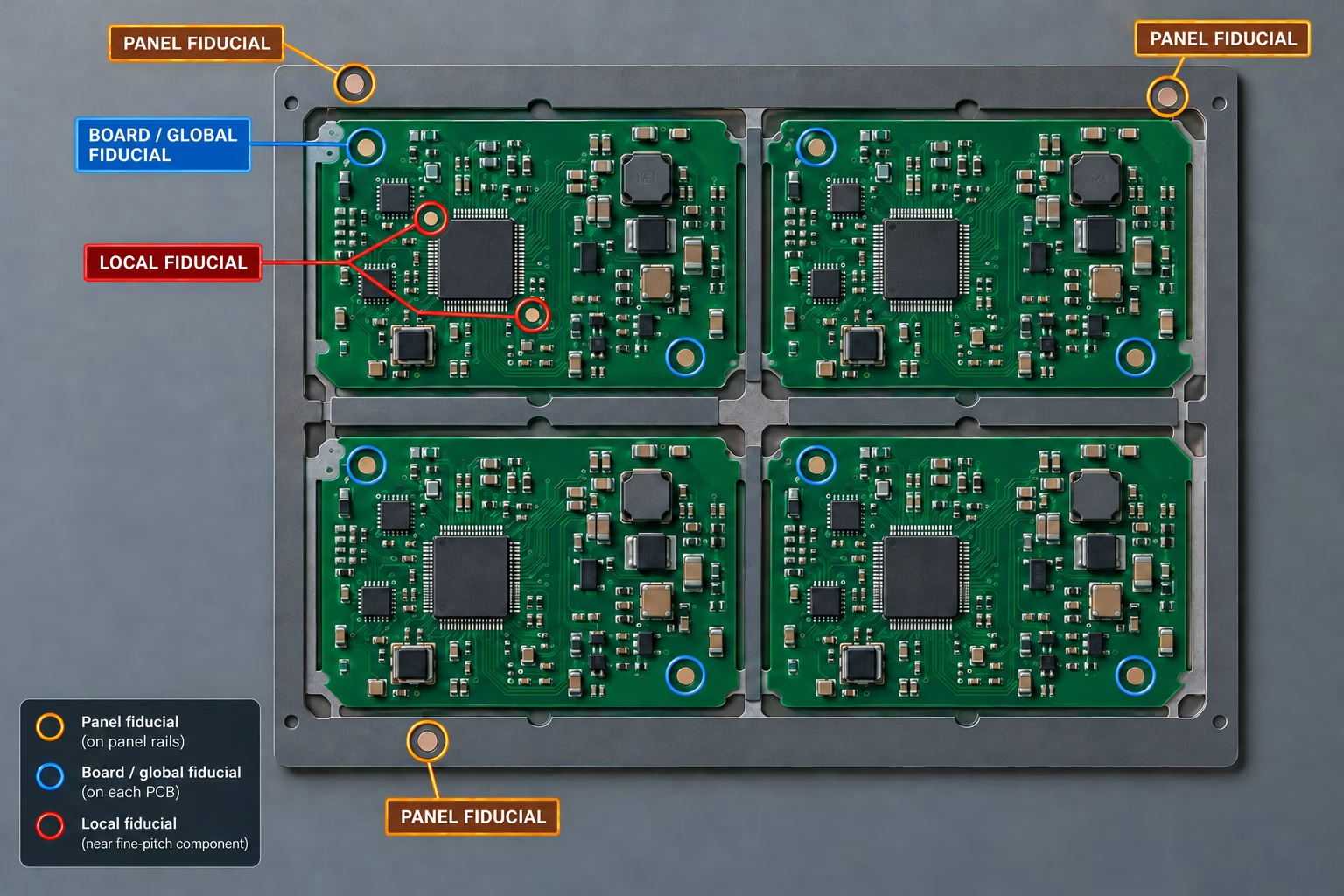
| Type | Alignment reference | Typical placement | When it matters |
| Panel | The coordinate system of the full production panel | Panel rails or waste border | Equipment handles several PCBs as one unit |
| Board or global | The coordinate system of one PCB | Widely separated corners or outer extents | The line aligns a standalone PCB or corrects individual PCB position within a panel |
| Local | One component land pattern or critical area | Close to and diagonally around the component | A placement-critical package needs a nearby optical reference |
This distinction answers a common counting question. Two local marks near a QFP do not replace the global references for the PCB. Likewise, three marks on a panel rail identify the panel datum, but they may not compensate for the positional variation of every routed board inside it.
OrinewPCB’s published panel design requirements usually place three panel fiducials in the middle of the edge rails. That is a house rule for OrinewPCB’s panel process, not a universal number for every assembly line.
How Many Fiducials Does a PCB Need?
There is no single count for every design because each alignment level has a separate job. A useful starting point is two marks for basic translation and rotation correction, or three non-collinear marks when the equipment uses an additional reference for scale or skew checks.
A SMEMA-based design guide gives the following logic:
- Two global fiducials: placed diagonally and as far apart as practical to correct X-Y and rotational offsets.
- Three global or panel fiducials: arranged as a wide triangle to provide an additional two-dimensional reference; whether the machine uses it for scale, skew, or other compensation depends on its alignment model.
- Two local fiducials: placed diagonally around a critical land pattern to correct local X-Y and rotation.
- One local fiducial: a space-limited fallback that can correct local translation but does not provide the same rotational reference as two marks.
For a conventional automated build, three non-collinear global marks are a robust layout baseline when space allows. Two widely separated global marks may be accepted by the assembly process. Panel fiducials and any local component fiducials are added for their own alignment tasks rather than deducted from that board-level count.
The marks should not form a straight line. A triangular arrangement gives the camera an unambiguous orientation and a two-dimensional reference. Spacing also matters: a small angular error is easier to detect when the marks are far apart.
PCB Fiducial Size and Clearance
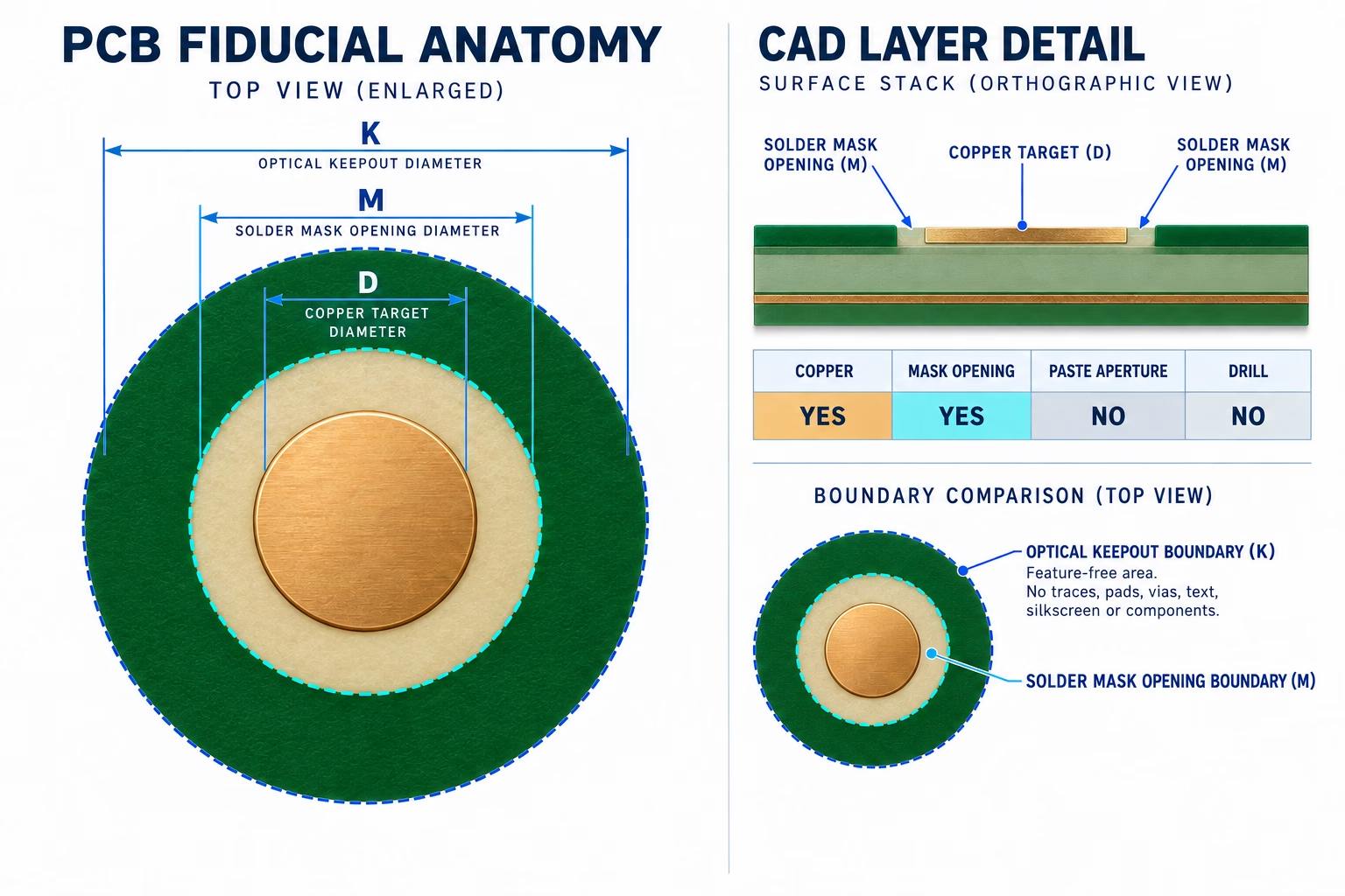
Fiducial size must describe three separate features: the copper target, the solder mask opening, and the clear optical area. A footprint labeled only “Fiducial 1 mm” is ambiguous unless the drawing says which feature the dimension controls.
PCB Fiducial Footprint Checklist
A PCB fiducial is an artwork feature, not a drilled tooling feature. The official KiCad 1 mm fiducial footprint provides a practical CAD example: it uses a surface-mount copper pad with a mask opening, but no drill and no paste-layer aperture. The dimensional ranges below come from the SMEMA-based design guide unless identified as an OrinewPCB panel specification.
| Footprint item | Recommended setup | Evidence or release check |
| Copper target | Solid filled circle, typically 1.0-3.0 mm diameter | Keep every mark recognized by one program the same size and finish |
| Solder mask | Expose the target and its specified clear area | Do not treat the mask opening as the full optical keepout unless the dimensions are actually equal |
| Paste layer | Do not create a solder paste aperture for the PCB fiducial | Standard KiCad fiducial footprints include copper and mask layers, not paste |
| Drill | None | A drilled feature is a tooling or mounting hole, not the copper artwork target described here |
| Optical keepout | Keep copper, vias, pads, text, and silkscreen out of the clear area | Minimum clear ring: target radius; preferred clear ring: target diameter |
| Assembly side | Place the footprint on every side assembled by automated equipment | Confirm that clamps, rails, and placed components cannot block the camera view |
| Design element | Generic guide | OrinewPCB panel specification | Release check |
| Copper target | Solid filled circle, 1.0-3.0 mm diameter | 1.0 mm diameter | Verify that the same recognition program sees a consistent target |
| Target consistency | No more than 25 microns size variation among marks on the same PCB | Use one consistent footprint unless the assembly drawing says otherwise | Do not mix target sizes without process approval |
| Mask opening | Keep solder mask off the target and the required clear area | 1.7 mm opening around the 1.0 mm panel target | State the mask diameter explicitly in the footprint or drawing |
| Optical clear area | Minimum clear ring width equal to the target radius; preferred ring width equal to the target diameter | Define separately when the project needs more clearance than the mask opening | Check copper, vias, pads, text, and silkscreen against the full keepout |
For a target diameter D, the generic rule above produces a minimum clear-area diameter of 2D and a preferred diameter of 3D. This is the full feature-free optical area, not just another name for the copper target. An assembler may use a different mask opening because its camera, lighting, finish, and image-processing settings are different.
The surface should be flat and provide consistent contrast. Bare or protected copper, nickel, tin, and HASL appear in published guidance, but a thick or uneven solder mound can make centroid detection less repeatable. Keep solder mask and silkscreen off the visible target. Use the same target geometry and finish across marks that one machine program will recognize.
How to Place PCB Fiducials
Place fiducials where the vision system can see them clearly and where their spacing gives a stable reference for the area being aligned.
- Use the assembled side. Put exposed fiducials on every side that will pass through automated component placement. A mark on the first side cannot be seen through the laminate when the camera aligns the second side.
- Spread global marks apart. Locate them near the outer extents of the usable board area. Two marks should normally be diagonal; three should form a large triangle rather than a line.
- Keep the camera background clean. Exclude same-side traces, copper pours, vias, pads, silkscreen, text, and component bodies from the optical keepout.
- Protect the transport area. Do not place a mark where a conveyor rail, clamp, tooling feature, or board support can cover it. One generic SMEMA-based guide reserves 7.62 mm (0.300 in) of transport clearance plus the mark’s required clear area, but the actual edge rule should follow the production panel and line.
- Place local marks close to the controlled land pattern. If the process calls for two, put them diagonally around the package and inside the camera’s usable field. They should remain outside the component body and paste area.
- Keep the artwork unambiguous. A test pad, via, logo dot, or nearby circular copper feature can create a competing target. Give the fiducial a visually distinct, repeatable background.
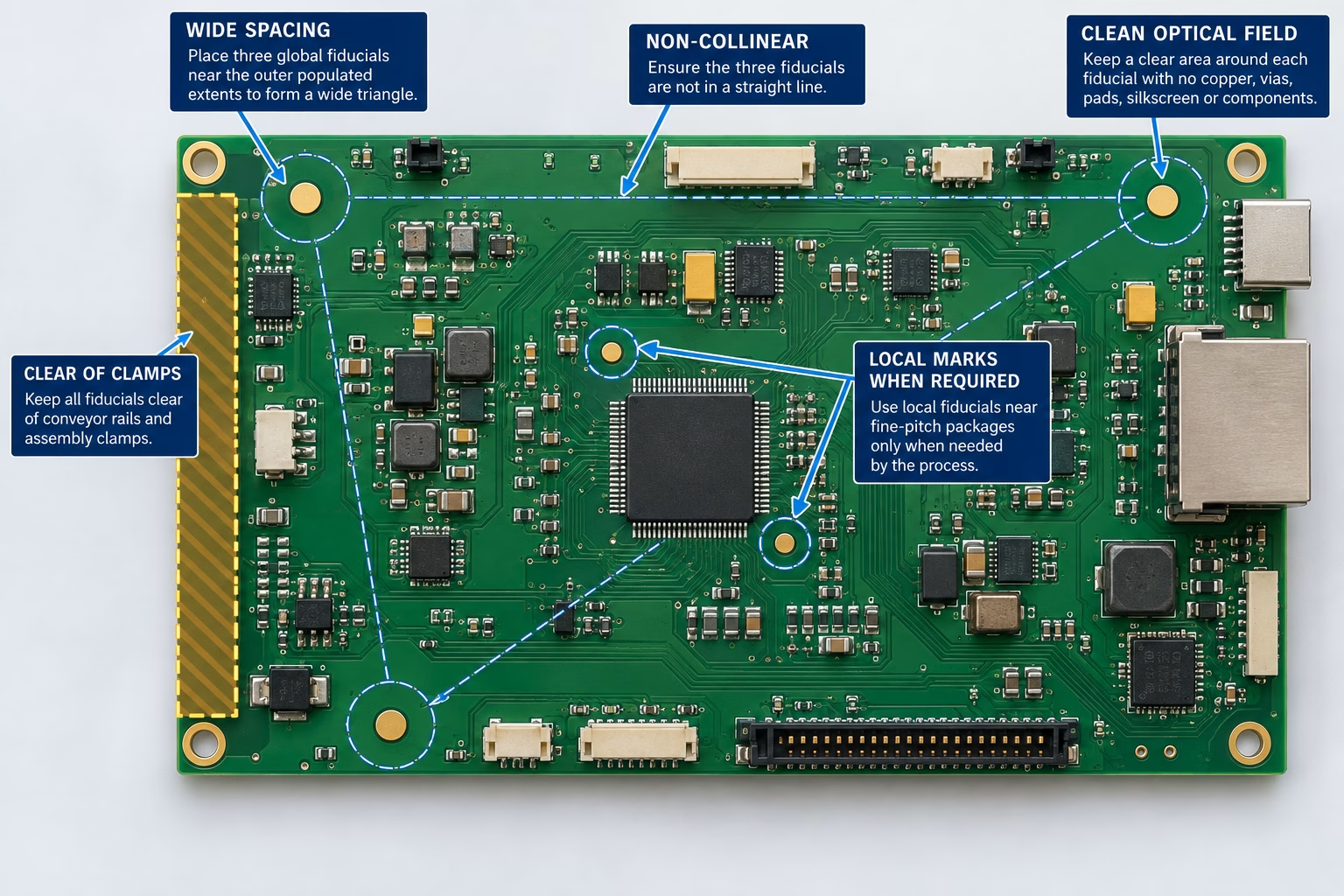
A PCB design rule check can verify copper spacing and mask geometry, but it does not know how a pick-and-place camera interprets the scene. Passing DRC does not prove that a mark is visible, unclamped, or compatible with the assembly program. Include fiducials in the same manufacturing review as panel rails, tooling holes, component courtyards, and stencil requirements. The PCB DFM checklist provides a broader handoff check for fabrication and assembly files.
Double-Sided and Irregular PCB Layouts
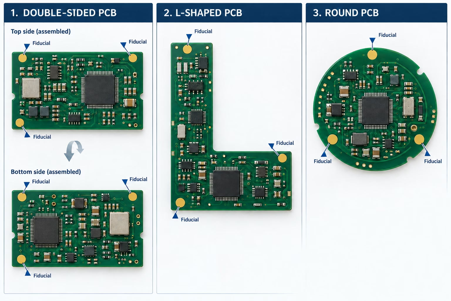
Each side of a double-sided automated assembly needs its own visible fiducial set. Keep the target size and clearance consistent between sides unless the assembly process specifies otherwise. The exact top-to-bottom coordinate relationship should follow how the line flips and programs the board; a copied visual pattern is not a substitute for that process definition.
For an L-shaped, T-shaped, round, or otherwise irregular PCB, distribute the global marks over the populated extents rather than forcing them into a rectangular corner pattern that covers only part of the design. Three non-collinear points still form the clearest reference. The marks must remain on material that survives routing and is accessible to the camera.
A component outside the triangle formed by three fiducials is not automatically unbuildable. The machine can still calculate a board coordinate transform. However, the farther a critical component lies beyond the reference area, the more any local board stretch or artwork distortion can affect the predicted position. Surround the populated region with the global marks when geometry permits, and add local references only where the process benefits from them.
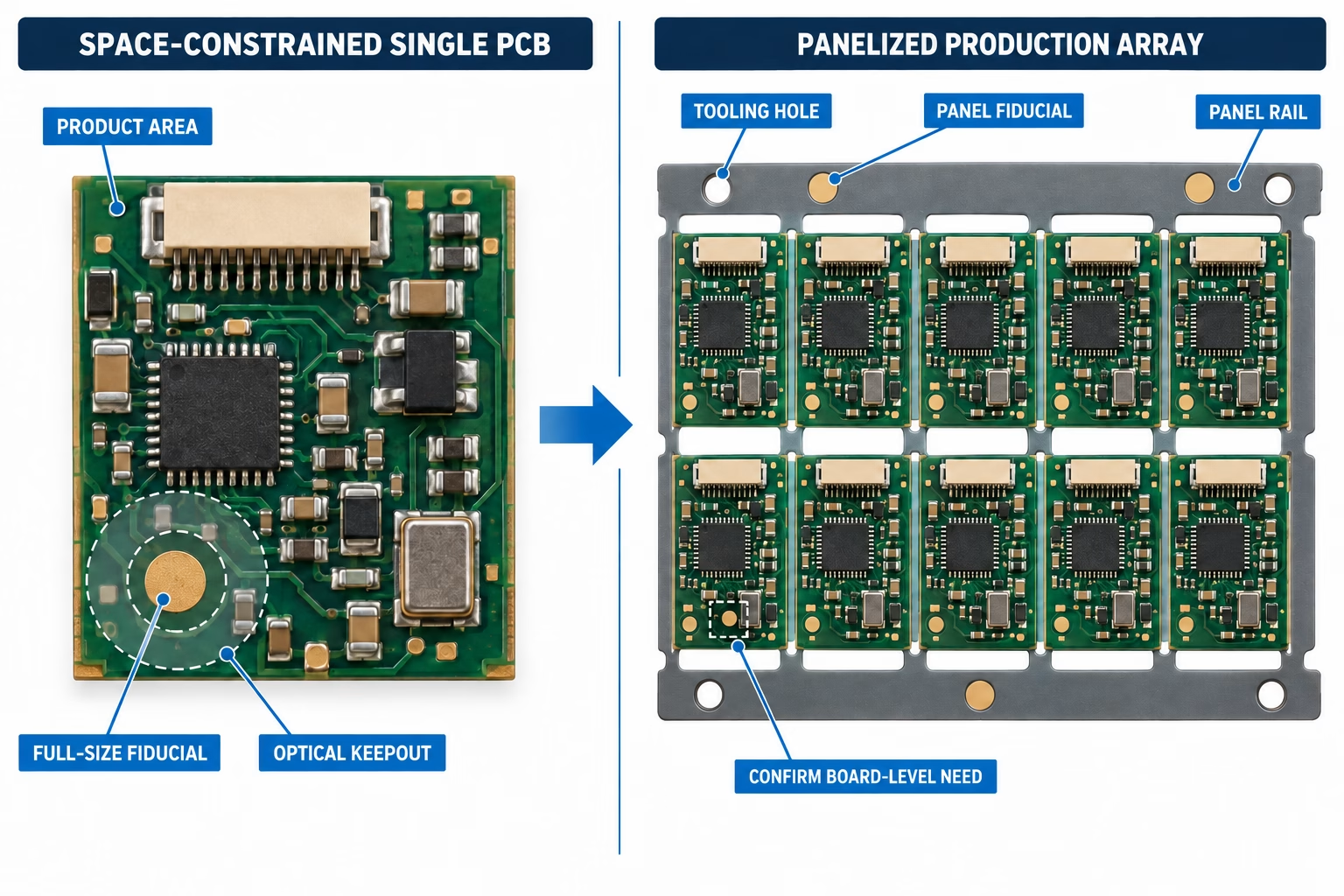
What If the Board Is Too Small for Standard Fiducials?
Panel fiducials can provide panel-level alignment, but they do not automatically replace every board-level or local alignment need. Start with the production setup before shrinking the marks or deleting them.
- Panelize the board. Rails provide room for panel fiducials and tooling features without consuming product area.
- Keep the panel and board tasks separate. Panel marks locate the carrier. Board marks may still be needed if routing, artwork registration, or local variation matters inside the panel.
- Review the component mix. A small board with relaxed-pitch parts may run from panel or global references. A large fine-pitch package can create a local accuracy requirement even when the PCB itself is tiny.
- Do not shrink by guesswork. A camera may recognize a smaller high-contrast mark, but that is an equipment capability, not a general design rule.
- Record an approved exception. If the production process accepts panel-only references, put that decision in the assembly notes or released manufacturing package so the next build does not depend on memory.
This is a good point for a focused DFM review. OrinewPCB can review the fiducial, panel rail, and assembly layout as part of an SMT assembly project before the files are released to production.
Common Fiducial Design Mistakes
Most fiducial problems come from unclear geometry, a blocked camera view, or using the wrong alignment level.
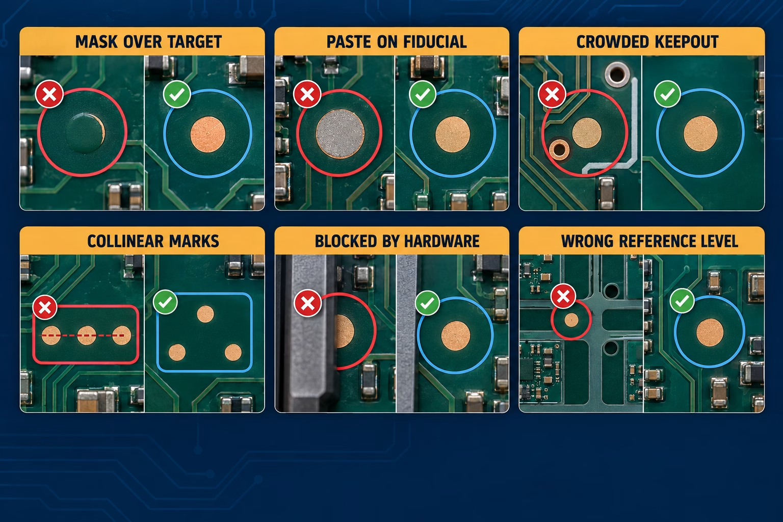
- One dimension for three features: The footprint name says 1 mm, but the drawing does not distinguish copper, mask opening, and optical keepout. Define all three.
- Marks in a straight line: Three collinear points do not provide the same two-dimensional geometry as a triangle. Move one mark onto the other axis.
- A crowded optical field: Same-side copper, silkscreen, text, paste, or nearby round pads can reduce contrast or confuse target recognition. Clear the full camera area.
- Marks hidden by production hardware: A perfectly drawn target is useless under a clamp or outside the camera travel. Check the panel and line setup.
- Panel marks counted as local marks: Each set aligns a different object. Define the panel, board, and component requirements independently.
- Local marks copied onto every footprint: Modern equipment may not need them for every QFN or BGA. Use local fiducials where component geometry and process capability justify the space.
- Assuming DRC is an assembly check: Electrical and mask rules do not evaluate image contrast, camera access, or coordinate strategy.
Conclusion
Start by identifying what must be aligned: the panel, the PCB, or a critical component area. Then choose the fiducial type, count, geometry, and clearance for that task. Two separated marks provide a basic position and rotation reference; three non-collinear marks provide a stronger board or panel reference; local marks are an additional process choice.
Use published dimensions as a starting point, not as a substitute for the actual assembly process. Keep copper diameter, solder mask opening, and optical keepout separate in the footprint and drawing. For OrinewPCB panels, the current published rule is usually three panel fiducials with a 1.0 mm copper target and 1.7 mm solder mask opening.
FAQ
How many fiducials are needed on a PCB?
Two widely separated global marks can correct X-Y offset and rotation. Three non-collinear marks provide an additional reference that some machines use for scale or skew checks. Count panel and local fiducials separately because they align different objects.
Are PCB fiducials needed for hand assembly?
Hand placement does not use a pick-and-place camera, so fiducials may not be needed for that step. Stencil printing, AOI, fabrication, or a future automated build may still use them. Decide from the full process rather than the placement method alone.
Can panel fiducials replace board fiducials?
Sometimes the assembly line can place all boards from the panel reference, but this is a process capability rather than an automatic substitution. Board-level marks may still be required to correct variation between individual circuits within the panel.
Can a trace run under a fiducial on the opposite PCB side?
The optical keepout applies to features visible on the surface being inspected, so an opposite-side trace normally does not enter the camera image through an opaque PCB. A fabricator or assembler may still define a multilayer keepout for its process. A clean DRC result confirms the programmed rules, not the assembly requirement.
What happens if fiducials are missing from the Gerber files?
Do not assume the board house will add them or that the assembly line can proceed unchanged. The assembler may accept another reference, modify the panel, request revised data, or limit the process. Resolve the method before fabrication because an unrecorded CAM edit can create a mismatch with the released design.
Should a PCB fiducial have a solder paste aperture?
Normally, no. A PCB fiducial needs an exposed copper target and a controlled optical background, not a solder deposit. For example, the KiCad standard fiducial footprint uses copper and solder mask layers without a paste-layer aperture. Stencil alignment features are specified separately by the stencil printer or supplier, so do not add a PCB paste aperture unless the production process explicitly calls for one.
Will the assembler add panel fiducials for me?
It may if it creates the production panel, but this is not automatic. Confirm who owns panel design before fabrication. When you provide panelized Gerbers, include the agreed panel marks; when the assembler panelizes the job, review its panel drawing or production data rather than assuming the CAM department will add the same geometry you intended.
Sources
- Solutions Manufacturing: Fiducial Mark Design Guidelines
- IPC-7351: Generic Requirements for Surface Mount Design and Land Pattern Standard
- Altium: Are Fiducial Marker Placements on PCBs Still Necessary?
- Fiducials in PCB Manufacturing
- KiCad: Fiducial_1mm_Mask2mm Footprint
- OrinewPCB: Panel Requirements for Assembly
- OrinewPCB: PCB DFM Checklist
Get Quote Free