PCB DFM Checklist: Quote-Ready Files Before PCB Manufacturing and Assembly
Use this PCB DFM checklist to catch file conflicts, stackup gaps, BOM issues, assembly risks, and test-access problems before quote, prototype, or production.
Get Your PCB Quote!
Table of Contents
Table of Contents
Direct answer: PCB DFM is the pre-build review that checks whether your board files describe one manufacturable product: the Gerbers, drill data, stackup, BOM, pick-and-place file, assembly drawing, and test requirements all have to agree before a quote or production order can move cleanly.
A clean CAD DRC is not a clean manufacturing release. CAD checks the rules you configured inside the layout tool. Manufacturer DFM checks whether this exact file package can move through CAM, fabrication, assembly, sourcing, inspection, and test without hidden assumptions.
The expensive problems rarely sit inside one file. They sit between files. A BOM may not match the pick-and-place file. A drawing note may conflict with the Gerber data. A polarity mark may be obvious on the schematic but missing from the assembly drawing. A test plan may arrive after layout is already locked.
This guide treats PCB DFM as a quote-readiness review, not a generic design-rule checklist. It separates DFM, DFA, and DFT, then maps the fabrication, assembly, file-control, and test-access gaps that stall quotes or turn into production findings.
Key Takeaways
- A clean CAD DRC is not a clean manufacturing release: CAD checks configured layout rules; DFM checks the released package against real fabrication, assembly, sourcing, and test constraints.
- The expensive failures sit between files: Gerber, drill, BOM, centroid, drawings, stackup notes, and test requirements must describe the same board.
- DFM, DFA, and DFT answer different questions: Fabrication, assembly, and testability risks should be reviewed separately before quote or production.
- Published limits are not universal rules: Confirm design limits against the manufacturer, material, copper, stackup, process route, and acceptance class for the actual build.
- A DFM report is a decision queue: Each finding should be revised, clarified, approved as a manufacturing assumption, or returned to the design authority.
The Quote-Ready Release Checklist: What to Review Before You Send Files
A quote-ready PCB package is not just a set of Gerbers. It is one controlled release that lets engineering, CAM, sourcing, assembly, and test work from the same assumptions.
| Check area | What to confirm | Why it matters | Owner |
| Release identity | One project name, revision, date, and file package | Prevents old files from being mixed into the build | Design owner |
| Fabrication data | Gerber, ODB++, IPC-2581, or agreed CAD/CAM output | Lets CAM review copper, mask, legend, drills, and board outline | PCB designer |
| Drill and route data | NC drill, plated and non-plated holes, slots, cutouts | Avoids missing holes, wrong plating assumptions, and mechanical fit issues | PCB designer |
| Stackup and material | Layer count, dielectric intent, copper, finish, impedance notes | Affects manufacturability, cost, lead time, and signal performance | Electrical engineer |
| Geometry | Trace, spacing, pad, via, annular ring, mask bridge, copper-to-edge | Confirms the layout fits the selected manufacturer’s process window | PCB designer and manufacturer |
| Panel and edge handling | Rails, breakaway method, tooling holes, fiducials, board orientation | Affects fabrication yield, SMT handling, and depaneling risk | Manufacturer and design owner |
| BOM | MPNs, quantities, reference designators, alternates, DNP lines | Prevents sourcing delays and wrong-part placement | Hardware and sourcing owner |
| Placement data | Pick-and-place / centroid file with rotation and side | Aligns machine programming with the assembly drawing | PCB designer |
| Assembly drawing | Polarity, variants, special instructions, connector orientation | Reduces manual interpretation on the line | Design owner |
| SMT process | Fiducials, stencil needs, fine-pitch parts, QFN/BGA access | Affects paste printing, placement, reflow, inspection, and rework | Assembly engineer |
| Test plan | Test points, ICT/FCT needs, programming, inspection criteria | Prevents late test-access changes and unclear acceptance criteria | Test engineer |
| DFM findings | Decision owner for each finding | Keeps quote and production from waiting on unresolved engineering questions | Project owner |
Read this table as the release gate. You do not need to memorize every possible PCB design rule; you need the right owner to answer each manufacturing question before money, tooling, components, and line time are committed.
What PCB DFM Actually Checks Before Quoting
PCB DFM means design for manufacturing in the context of printed circuit boards. At bare-board level, it asks whether the PCB can be fabricated consistently by the selected manufacturer. On a real order, the review usually widens into assembly, sourcing, and test because the board does not ship as an isolated layout file.
The manufacturer is asking a sharper question: can this exact release package move through this supplier’s CAM, fabrication, assembly, inspection, and test process without unclear assumptions?
CAD DRC is not the same as manufacturer DFM
Design rule checks inside PCB CAD software are only as good as the rule set you configured. If the rules do not match your target manufacturer, stackup, copper weight, drill structure, solder mask process, or assembly route, a “clean” DRC result can still produce manufacturing questions.
Manufacturer DFM review catches different categories of risk:
- Fabrication geometry that is too close to the shop’s process limits.
- Drawing notes that conflict with exported manufacturing data.
- Stackup or impedance expectations that are missing or ambiguous.
- Board shapes or panel plans that create handling problems.
- Assembly details that are not visible in the bare-board design files.
Key point: DFM is a release review, not a layout cleanup step.
DFM should happen before RFQ, prototype release, and production release
Run DFM before the design is treated as final. At quote stage, it tells the manufacturer what is being priced. At prototype stage, it catches issues before a design spin. At production release, it keeps small prototype assumptions from becoming repeatable production problems.
If your supplier cannot quote without several engineering questions, the problem is not always supplier responsiveness. Sometimes the release package simply does not define the real build yet.
What a DFM report usually contains
A PCB DFM report is a list of manufacturing findings, file conflicts, risk notes, suggested corrections, or quote assumptions. A good report should tell you what was found, where it appears, why it matters, and what decision is needed.
Not every DFM finding means the board is wrong. Some findings are hard stops. Others are manufacturability cautions, cost drivers, or assumptions the manufacturer needs you to approve.
The DFM/DFA/DFT Boundary Map: What Each Review Checks
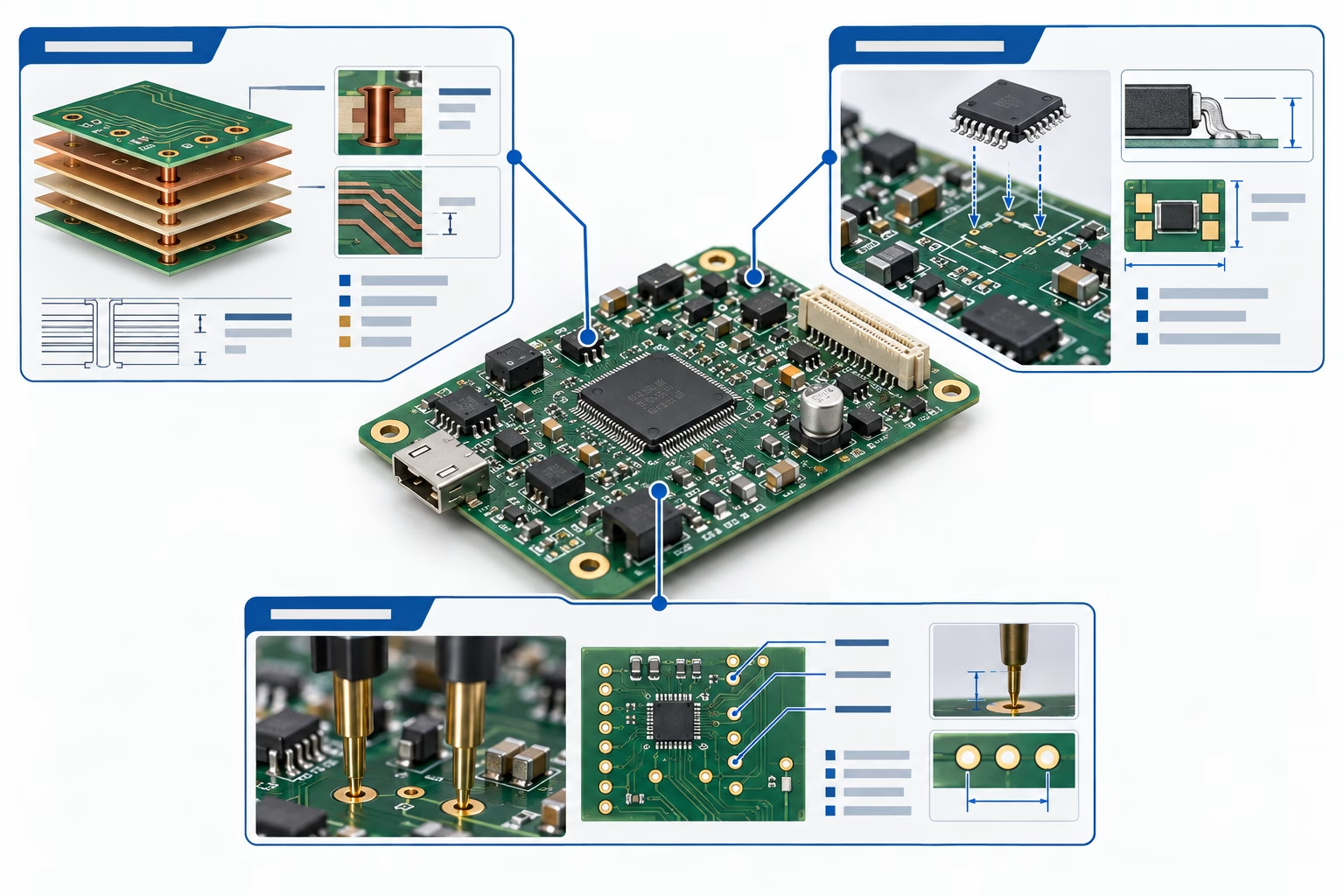
DFM, DFA, and DFT are related, but they do not check the same risk. Treating them as one review is how gaps slip through.
| Review type | What it checks | Typical files needed | What it means for your build |
| DFM | Bare-board manufacturability | Fabrication data, drill files, stackup, material notes, fab drawing | Whether the PCB can be fabricated as released |
| DFA | Assembly readiness | BOM, pick-and-place data, assembly drawing, polarity notes, stencil needs | Whether components can be placed, soldered, inspected, and handled |
| DFT | Testability | Test point plan, netlist, functional test needs, programming notes, acceptance criteria | Whether defects can be found and verified after assembly |
DFM: bare board fabrication risk
DFM focuses on the printed circuit board itself. It looks at the manufacturability of copper features, holes, layer registration, solder mask, silkscreen, board outline, stackup, materials, surface finish, and panelization.
The key DFM question is: can this PCB be fabricated repeatably by the intended shop, using the intended process, without hidden assumptions?
DFA: component placement and soldering risk
DFA means design for assembly. In PCBA work, it checks whether components can be sourced, placed, soldered, inspected, reworked if needed, and handled through the assembly process.
DFA cares about details that may not matter to bare-board fabrication: component orientation, polarity marks, spacing for placement nozzles, stencil apertures, thermal balance, tall components, connectors, hand-solder operations, and whether the assembly drawing matches the BOM and placement file.
DFT: test access and verification risk
DFT means design for test. It checks whether the finished board can be inspected, powered, programmed, measured, and accepted with the agreed test method.
DFT is frequently left too late. If test points, fixture access, programming headers, or functional test requirements are not considered during layout, the final board may be buildable but hard to verify.
The Fabrication DFM Risk Table
Fabrication DFM starts with the bare board. The review should confirm that the exported manufacturing data, drawing notes, and design intent all describe the same PCB.
Do not treat web checklist values as universal rules. The correct limit depends on your manufacturer, material, copper, board class, layer structure, and process route.
| Fabrication area | Check | Common issue | What to clarify with the manufacturer |
| Stackup | Layer count, dielectric structure, copper, impedance intent | Stackup is implied but not documented | Ask whether the proposed stackup meets electrical and fabrication needs |
| Material | Base material, Tg, halogen-free need, RF or high-speed laminate | Material named loosely or not available in the required lead time | Confirm material availability and approved alternates |
| Copper geometry | Trace width, spacing, copper balance, copper-to-edge | CAD rules do not match process limits | Confirm against the specific capability for that build |
| Drilling | Mechanical holes, vias, slots, plated/non-plated status | Hole table conflicts with drill file or drawing | Confirm drill map, plating status, and slot requirements |
| Annular ring and vias | Pad size, via type, breakout risk, filled or capped vias | Via treatment is assumed but not specified | Confirm via process and inspection expectations |
| Solder mask | Mask dam, clearance, via tenting, exposed copper | Mask slivers or tenting assumptions create assembly risk | Confirm solder mask rules and whether vias should be tented |
| Silkscreen | Reference designators, polarity, component outlines | Text overlaps pads or polarity is unclear | Confirm what legend will remain readable after manufacturing |
| Board outline | Slots, cutouts, tolerances, controlled edges | Mechanical drawing and board outline data disagree | Confirm the controlling file and mechanical tolerance |
| Panelization | Rail width, tooling, fiducials, breakaway method | Design ships as a single board but assembly needs a panel | Ask whether the manufacturer or designer should control panel design |
| Fabrication notes | Finish, IPC class, impedance, special processing | Notes are copied from old projects and no longer apply | Remove old notes and confirm the actual release requirements |
Stackup, material, thickness, copper, and impedance intent
A PCB stackup is not only a layer count. It defines the relationship between signal layers, planes, dielectric materials, copper, thickness, impedance expectations, and manufacturability.
Use IPC design standards and the manufacturer’s current capability together, not one in isolation. IPC-2221 may tell you how printed boards are generally designed; the shop’s process window tells you whether this stackup, copper, drill structure, and material set can be built on the requested lead time.
If impedance matters, do not only write “controlled impedance” in a drawing note. State the target nets, target impedance, tolerance, stackup assumption, and whether the manufacturer may adjust trace geometry to hit the measured requirement. The calculator value is the starting point, not the proof.
Trace, spacing, via, drill, slot, and annular ring checks
Many DFM problems appear when a design sits near a process edge. A board may pass CAD checks but still need CAM review because copper weight, plating, drill structure, solder mask, and material all interact.
Do not treat published minimums as the design target. If a geometry is close to the manufacturer’s stated capability, ask whether it is routine production, an advanced process, or a cost and yield risk. That answer matters more than the number on a generic checklist.
Solder mask, silkscreen, board edge, and panelization checks
Solder mask and silkscreen are easy to treat as cosmetic layers. They are not. Mask clearances affect solder bridging risk. Silkscreen affects placement and inspection. Board edge design affects depaneling and mechanical fit. Panelization affects SMT handling and throughput.
If your board needs a specific breakaway method, rail location, fiducial strategy, or edge quality, define it before quote. If you expect the manufacturer to design the panel, say so and define the assembly constraints.
Fabrication drawing and notes that prevent assumptions
A fabrication drawing should remove ambiguity, not create it. Check old template notes carefully. A note copied from a previous project can override the current Gerber or ODB++ package in exactly the wrong direction.
Before release, confirm that finish, board thickness, stackup, copper, solder mask color, silkscreen color, controlled impedance, IPC class, special testing, and inspection requirements are intentional and current. Old notes are not harmless; they are instructions.
The Assembly DFA Readiness Table
Assembly DFA checks whether the design can move through component sourcing, paste printing, placement, soldering, inspection, rework, and final test without preventable friction.
A board can be fabricable and still be difficult to assemble. DFA is where the PCB stops being a bare board and becomes a production object.
| Assembly area | Check | Why it matters | Fix before release |
| Footprints | Land pattern, package match, pin count, exposed pad | Wrong footprints can stop assembly or cause solder defects | Compare footprints against the selected component datasheet |
| Polarity | Diodes, LEDs, ICs, connectors, electrolytic capacitors | Wrong orientation can destroy parts or fail test | Make polarity visible in silkscreen and assembly drawing |
| Placement | Spacing, height, orientation, nozzle access | Dense placement can slow assembly and inspection | Review component keepouts and placement access |
| Fiducials | Global and local fiducials if required | Placement machines need accurate alignment | Add fiducials early, especially for fine-pitch work |
| Stencil and paste | Aperture needs, fine-pitch parts, exposed pads | Paste volume affects bridging and insufficient solder | Flag special stencil needs before assembly |
| Thermal balance | Large copper, heat sinks, mixed thermal mass | Reflow can become uneven | Review with assembly engineer before release |
| BGA/QFN | Hidden joints, X-ray needs, escape routing | Visual inspection may not see joint quality | Define inspection and rework expectations |
| Through-hole | Connector fit, lead length, soldering method | Mixed technology affects process route | Separate SMT and THT needs clearly |
| Variants | DNP parts, population options, customer options | Wrong variant can be built from a correct BOM | Create variant-specific BOM and assembly notes |
Footprints, polarity marks, and assembly drawings
Start with the footprint. A BOM can name the correct component while the footprint still fits a different package. The land pattern, pin count, exposed pad, courtyard, and package orientation need to agree with the actual part being purchased.
Polarity should be clear in more than one place. Use the assembly drawing as the controlling human-readable document, and make sure the silkscreen does not create a second, conflicting interpretation.
Component spacing, height, access, and placement orientation
Component placement affects machine access, rework access, inspection visibility, and mechanical fit. Crowding parts together may save board area but create assembly cost or yield risk.
Look closely at tall components, connectors, shields, heat sinks, edge parts, fine-pitch ICs, and parts placed near breakaway tabs. These are the locations where a design that looks compact in CAD can become awkward on the line.
BGA, QFN, fine-pitch, and hidden-joint review
BGA and QFN packages need extra attention because many solder joints cannot be inspected visually. The design should define escape routing, solder mask strategy, paste requirements, thermal pad treatment, and inspection expectations.
If the board has high-reliability requirements, do not leave hidden-joint inspection as an informal assumption. State what level of inspection, test, and acceptance evidence is expected for the build.
Fiducials, stencil/paste, and reflow considerations
Fiducials, stencil design, paste volume, thermal mass, and reflow profile interact. Watch this closely when the board mixes large thermal pads, small passive parts, heavy copper areas, connectors, and fine-pitch ICs.
Ask the assembly team which details they want before release. A short review before quoting is cheaper than discovering that the paste strategy or fiducial plan needs layout changes after files are frozen.
Through-hole and mixed-technology assembly checks
Through-hole parts can drive manual labor, soldering method, fixture needs, and inspection flow. If the board uses connectors, transformers, relays, switches, large capacitors, or mixed SMT/THT assembly, mark them clearly in the drawing and BOM.
Do not assume every through-hole part follows the same soldering path. Selective soldering, wave soldering, hand soldering, and press-fit processes have different design constraints.
The File-Conflict Crosswalk: BOM, Gerber, Pick-and-Place, and Drawings
The fastest DFM review starts with a clean file package. The most frustrating review starts with technically correct files that disagree with each other.
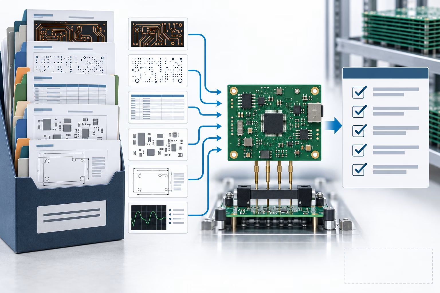
Gerber remains the widely used transfer format for fabrication data: copper, solder mask, legend, drill, route, and board outline. Newer Gerber attributes can carry more manufacturing metadata. Even so, a Gerber package by itself does not replace a BOM, assembly drawing, stackup note, centroid file, or test plan. It tells the fabricator how to make the bare board; it does not tell the assembler which parts to place or the test engineer how the finished PCBA will be accepted.
| File | Required fields | Common mismatch | Who should approve |
| Fabrication export | Copper, mask, legend, paste if needed, board outline, drill/route | Export date or revision differs from drawing | PCB designer |
| NC drill | Tool sizes, plated/non-plated status, slots | Drill file does not match hole table | PCB designer and manufacturer |
| Fabrication drawing | Stackup, material, finish, thickness, tolerance, special notes | Old notes conflict with current design | Design authority |
| BOM | MPN, manufacturer, quantity, refdes, description, alternates, DNP | BOM quantity does not match placement file | Hardware and sourcing owner |
| Pick-and-place | Refdes, X/Y, rotation, side, package | Rotation or side conflicts with assembly drawing | PCB designer and assembly engineer |
| Assembly drawing | Polarity, variants, special processes, mechanical orientation | Drawing lacks enough detail for human inspection | Design owner |
| Test requirements | Programming, ICT/FCT, visual inspection, acceptance notes | Test is requested but access points are not designed | Test engineer |
| Readme / release note | Revision, open questions, intended build quantity, contact owner | Supplier does not know which file controls | Project owner |
BOM fields that reduce sourcing delays
A quote-ready BOM should name the actual manufacturer part number when possible. It should also show reference designators, quantity, description, approved substitutes, DNP lines, and any customer-controlled or consigned parts.
Treat the BOM as a sourcing instruction, not a parts wish list. If substitutes are acceptable, define the approval rule. If they are not, mark the line as controlled before the buyer or manufacturer has to guess.
Pick-and-place data and centroid alignment
Pick-and-place data should agree with the assembly drawing and BOM. Check component side, reference designator, X/Y location, rotation, and package. If your CAD tool uses a rotation convention that differs from the assembly house, the manufacturer may need to normalize the data before programming.
Include an assembly drawing that makes orientation visually clear. The machine file and the human-readable drawing need to tell the same story.
Assembly drawing, polarity, variants, and DNP items
Variant control is one of the simplest ways to prevent assembly confusion. If one PCB supports multiple product options, create a release package for each population option or make the build option unmistakable.
Use DNP consistently. A part marked DNP in the BOM should not appear as a placed part in the pick-and-place file unless the file is clearly variant-specific.
One release archive, one revision ID
Before uploading files, create one archive for the build. Remove old exports, screenshots, draft drawings, and obsolete BOMs. Put the revision ID in the file name or release note and repeat it inside the package.
Decision rule: if a manufacturer has to choose between two files, the release is not yet controlled.
The DFM Finding Decision Queue: Common Issues and Corrections
Common PCB DFM issues usually come from ambiguity, not incompetence. The design may be electrically correct while the released manufacturing package leaves too many choices open.
A DFM report is not a rejection letter. It is a decision queue: revise the file, clarify the requirement, approve the manufacturing assumption, or send the finding back to the design authority.
| Issue | Why it happens | Corrective action | Who approves |
| Conflicting files | Old exports remain in the release package | Re-export and send one controlled archive | Project owner |
| Missing stackup | Layer count is known but construction is not defined | Ask manufacturer for stackup proposal or provide target stackup | Electrical engineer |
| Unclear impedance | Controlled nets are not named or tolerance is missing | Define target nets and expected impedance requirement | Electrical engineer |
| Geometry near limits | CAD rules are not matched to the actual supplier | Review against manufacturer capability before release | PCB designer |
| Drill conflict | Hole table, drill file, and drawing disagree | Identify controlling data and regenerate package | PCB designer |
| Solder mask risk | Mask openings or via tenting assumptions are unclear | Specify via treatment and confirm mask manufacturability | PCB designer and manufacturer |
| Polarity ambiguity | Silkscreen and drawing do not clearly show orientation | Add clear polarity marks and drawing notes | Hardware engineer |
| BOM ambiguity | MPNs, alternates, DNP, or lifecycle status are incomplete | Normalize BOM and approve substitutes before buying | Sourcing and engineering |
| BGA/QFN inspection gap | Hidden joints need inspection planning | Define inspection and test expectations before quote | Quality or test owner |
| Test access gap | Test points are not included before layout is frozen | Add test access or change the test strategy | Test engineer |
FAQ
What is a DFM report for PCB design?
A PCB DFM report is a set of manufacturability findings created after a manufacturer reviews your released design package. It may include file conflicts, fabrication risks, assembly concerns, missing requirements, suggested corrections, and assumptions that need approval before quote or build. A good report tells you what was found, why it matters, and who needs to decide.
What are DFM and DFT in PCB design?
DFM checks whether the PCB can be manufactured by the selected process. DFT checks whether the finished board can be tested, programmed, inspected, or functionally verified. DFM helps the board get built. DFT helps the finished assembly prove it works. A board can pass DFM and still fail DFT if the layout never left room for test access.
What are common DFM issues found in PCBs?
Common PCB DFM issues include mixed-revision files, conflicting drawing notes, unclear stackup, geometry near process limits, solder mask concerns, footprint or polarity mismatch, incomplete BOM data, and missing test access. Most are not exotic board failures. They are release-control gaps that can be corrected before fabrication starts.
What is the 3W rule in PCB routing?
The 3W rule is a layout guideline often discussed for spacing between traces in certain signal-integrity contexts, but it is not a universal PCB manufacturing rule. Do not use it as a substitute for impedance design, electromagnetic review, or your manufacturer’s actual spacing capability.
Ready to Send a Quote-Ready PCB Package?
If your Gerber, drill file, BOM, centroid, assembly drawing, and test notes do not tell the same story, the quote will be built on assumptions. Send the full release package for DFM/DFA review before those assumptions turn into tooling, sourcing, assembly, or test delays.
References & Sources
IPC Document Revision Table – IPC
IPC Design Standards – IPC
Meet Your Standards – IPC
Official Gerber Format Website – Ucamco
Ucamco File Formats – Ucamco
Ucamco Downloads – Ucamco
Related Articles

Get Quote Free