How to Choose Between 2-Layer and 4-Layer PCBs
Compare 2-layer and 4-layer PCBs by routing density, return paths, EMI, impedance, power distribution, board size, and total project cost.
Get Your PCB Quote!
Table of Contents
- 2-Layer vs. 4-Layer PCB: Quick Comparison
- How Layer Count Changes Routing and Return Paths
- The Factors That Should Decide Your Layer Count
- When a 2-Layer PCB Is the Better Choice
- When to Move to a 4-Layer PCB
- Choosing a Practical 4-Layer Stackup
- How Cost Changes Between 2 and 4 Layers
- A Five-Step Way to Choose
- Conclusion
- FAQ
- Source
Table of Contents
- 2-Layer vs. 4-Layer PCB: Quick Comparison
- How Layer Count Changes Routing and Return Paths
- The Factors That Should Decide Your Layer Count
- When a 2-Layer PCB Is the Better Choice
- When to Move to a 4-Layer PCB
- Choosing a Practical 4-Layer Stackup
- How Cost Changes Between 2 and 4 Layers
- A Five-Step Way to Choose
- Conclusion
- FAQ
- Source
A 2-layer PCB is usually the right choice when the circuit routes comfortably, the board has enough space, and you can preserve a useful ground reference. Move to four layers when routing starts cutting up the ground area, the board must grow just to fit traces, or critical signals need a more predictable reference structure.
The decision should not come from component count or clock frequency alone. Routing density, signal edge rate, return paths, controlled impedance, power distribution, board size, EMC margin, and total project cost all matter. Four layers make these requirements easier to manage, but extra layers do not repair poor placement or routing automatically.
2-Layer vs. 4-Layer PCB: Quick Comparison
This table compares typical boards under similar functional and mechanical requirements. A specific design may use a different stackup or assign its layers differently.
| Decision factor | 2-layer PCB | 4-layer PCB |
| Copper structure | Top and bottom copper, both normally shared by signals, power, and ground | Four copper layers, often with one or two internal reference or power layers |
| Routing space | Suitable when the netlist fits without badly fragmenting ground copper | More freedom for dense placement, package escape, and compact board outlines |
| Return paths | Can be good if one layer remains largely continuous or both sides use well-stitched ground copper | Easier to provide a solid reference close to critical surface traces |
| Controlled impedance | Possible, but the required trace width may be inconvenient on a thick board | Usually easier because signal-to-reference spacing can be smaller and better controlled |
| Power distribution | Uses traces and pours that compete with signal routing | Can use an internal plane or wide power regions, depending on the stackup |
| EMI and signal integrity | More dependent on careful placement, short routes, and unbroken return paths | Usually provides more margin, but only with a suitable stackup and layout |
| Fabrication | Simpler process and usually lower bare-board cost | Requires inner-layer processing, alignment, and lamination |
| Best fit | Simple, spacious, cost-sensitive, or low-density designs | Dense, compact, interface-heavy, impedance-controlled, or EMC-sensitive designs |
The practical goal is not to use the fewest layers at any cost. It is to use the lowest layer count that meets the electrical and mechanical requirements with reasonable design margin.
How Layer Count Changes Routing and Return Paths
The main electrical advantage of four layers is not extra copper alone; it is the ability to place critical signals next to a continuous reference plane.
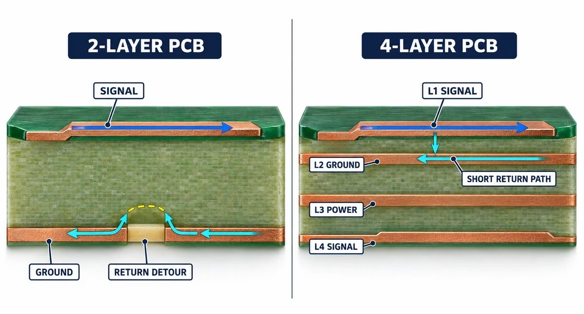
Every signal current flows in a loop. The outgoing current travels along the signal trace, while the return current completes the loop through ground or another reference conductor. At higher frequencies, the return current tends to concentrate close to the signal path when a continuous reference plane is available. This keeps the loop area and its inductance small.
If a trace crosses a slot, split, or heavily fragmented ground region, the return current must detour around the discontinuity. That larger loop can increase radiation, susceptibility, and impedance disturbance. Texas Instruments illustrates this relationship in its Practical PCB Design Rules, while Microchip explains why a complete ground plane reduces loop area in its guidance on current loops and signal grounding.
A 2-layer board can still provide a good return structure. One common approach is to place most components and signal routing on one side while keeping the other side as continuous a ground layer as possible. When both sides must carry routes, ground pours and stitching vias can help, but every trace and clearance creates a gap in the copper. As the layout becomes denser, maintaining a short return path becomes increasingly difficult.
On a 4-layer board, an internal ground layer can remain intact while outer layers carry components and signals. This does not guarantee good EMC. A signal routed over a split power region, a poorly handled layer transition, or a long route through a noisy area can still cause trouble. Layer count creates the opportunity for a better reference structure; placement, stackup, and routing must use it correctly.
The Factors That Should Decide Your Layer Count
Choose the layer count by evaluating routing density, board size, signal edges and interfaces, reference-plane continuity, power distribution, and EMC margin together. No universal component count, net count, or clock-frequency threshold separates a 2-layer board from a 4-layer board.
Routing Density and Board Area
Start with the required board outline, connector locations, and package pitches. If a two-layer layout fits with comfortable trace widths and spacing while preserving useful ground copper, adding layers may provide little benefit.
Four layers become more attractive when routes repeatedly block one another, fine-pitch packages are difficult to escape, or the board outline must grow mainly to create routing channels. A larger 2-layer PCB may also reduce the expected cost advantage by using more panel area or requiring a larger enclosure.
Signal Edge Rate and Interfaces
Do not classify a board as “slow” from clock frequency alone. A low-frequency bus can still be driven by a device with fast voltage transitions, and those fast edges contain higher-frequency energy. Trace length, driver edge rate, receiver tolerance, termination, and the quality of the return path determine whether interconnect behavior matters.
Interface and component layout guides are more useful than a generic MHz rule. For example, Texas Instruments recommends a four-layer stackup for most TM4C129x designs, while also listing conditions under which a two-layer stackup may be acceptable in its TM4C129x system design guidelines. That recommendation belongs to the device and interfaces covered by the document; it should not be turned into a universal threshold for every PCB.
Return-Path Continuity and EMI
Check where the return current will flow for clocks, switching nodes, communication interfaces, and other fast-changing signals. If those traces can stay over continuous reference copper on a two-layer board, two layers may be sufficient. If routing repeatedly cuts the ground structure or forces long return detours, four layers provide a cleaner solution.
EMC certification is not proof that four layers are mandatory, and four layers are not proof that a product will pass. Cables, enclosure openings, switching loops, decoupling, filters, placement, and stackup all contribute. The layer decision changes how easily the PCB can control these paths and how much design margin is available.
Controlled Impedance
Controlled impedance depends on trace width and thickness, dielectric properties, and the distance to the reference plane. A 2-layer board can support controlled-impedance routing, but on a standard thick board the reference plane may be far enough away that the required trace becomes impractically wide.
Texas Instruments notes this limitation for 2-layer low-power RF designs and explains that careful placement, routing, and a thinner board can produce performance comparable to a 4-layer implementation in the conditions covered by AN098. Four layers usually make impedance geometry easier because a signal layer can be separated from its reference plane by a thin dielectric. The actual trace dimensions must still come from the fabricator’s stackup and an appropriate field solver or impedance calculation; this PCB impedance-control guide explains the geometry and calculation inputs in more detail.
Power Distribution
Simple circuits with one or two modest power rails can often use wide traces and pours on a 2-layer board. Local decoupling still matters, and power routing should not destroy the ground return structure.
A 4-layer board offers more options. One internal layer may distribute power, or power can share an outer layer while both inner layers provide ground references. The better choice depends on the number of rails, transient current, sensitive circuits, and which signal layers need an adjacent reference. A power plane is useful only when its shape and relationship to the rest of the stackup support the design.
Mechanical and Revision Constraints
Four layers can help fit the same function into a smaller outline, but layer count does not directly determine board thickness or mechanical strength. Fabricators offer multiple finished thicknesses and copper constructions for both 2-layer and 4-layer boards.
Also consider prototype access and likely revisions. A simple 2-layer board may be easier to inspect, cut, and patch during early development. A compact 4-layer layout may take less time to route and provide more electrical margin, but internal connections are less accessible for manual modification. Neither option is automatically better; the product stage matters.
When a 2-Layer PCB Is the Better Choice
Use two layers when the layout fits comfortably and you can keep a useful ground reference without forcing long detours, narrow bottlenecks, or a larger enclosure.
A 2-layer board is a strong candidate when:
- The circuit has low routing density and generous board area.
- Critical traces are short, and their return paths remain clear.
- There are no demanding interfaces that require tightly controlled geometry, or those interfaces can be implemented within a verified 2-layer stackup.
- Power distribution is simple enough to route without fragmenting ground.
- EMC requirements are manageable with disciplined placement, routing, filtering, and enclosure design.
- Lowest bare-board cost or easy prototype modification has real value.
Two layers are not limited to trivial circuits. TI’s RF guidance shows that a carefully designed 2-layer board can achieve comparable performance to a 4-layer design for the specific low-power RF conditions it covers. The tradeoff is design freedom: the placement, board thickness, ground continuity, and RF routing require closer control.
When to Move to a 4-Layer PCB
Move to four layers when routing repeatedly breaks up ground, the board grows mainly to fit traces, or critical interfaces need a more predictable reference structure.
Strong signs that four layers are justified include:
- Dense placement or fine-pitch packages leave too little space for clean signal, ground, and power routing on two surfaces.
- A two-layer trial requires many ground-plane cuts, long detours, or excessive vias.
- Controlled-impedance interfaces need a practical, repeatable trace geometry.
- Fast-edged signals, RF paths, sensitive analog circuits, or mixed-signal sections need cleaner return paths and better isolation.
- The product has limited board area or a fixed enclosure.
- EMC margin is important enough that another layout spin or test cycle would cost more than the additional fabrication complexity.
Use these signs together. A single microcontroller, a particular clock frequency, or one high-current net does not independently prove that four layers are required. Conversely, a board can have relatively few components and still benefit from four layers if it contains a demanding interface or must fit into a small space.
Choosing a Practical 4-Layer Stackup
A common signal–ground–power–signal stackup is a starting point, but the best arrangement depends on which signal layers need a solid adjacent reference and how power is routed.
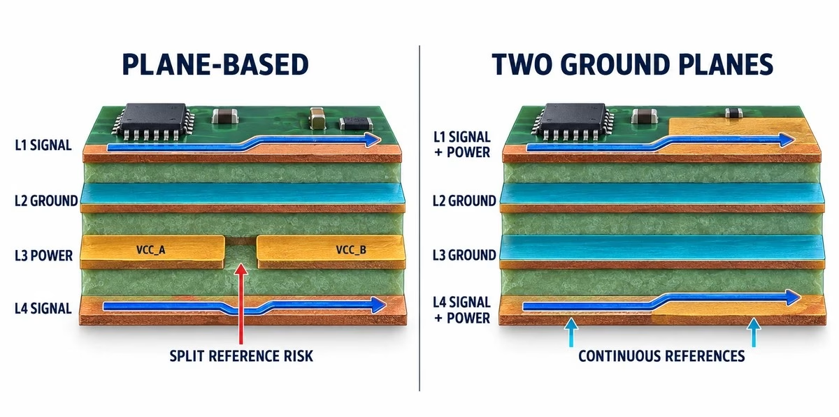
Two useful starting configurations are:
| Layer | Common plane-based stackup | Two-ground-plane stackup |
| L1 | Signal and components | Signal, power, and components |
| L2 | Solid ground | Solid ground |
| L3 | Power plane or power regions | Solid ground |
| L4 | Signal and components | Signal, power, and components |
The first arrangement gives the top signal layer an adjacent ground reference and provides convenient power distribution. However, bottom-layer signals may reference the power layer. If that power plane is split into several rails, a critical bottom trace can cross a reference discontinuity unless routing is planned carefully.
The second arrangement gives both outer signal layers an adjacent ground reference. Power is routed as traces or pours on the outer layers, so the design gives up a dedicated power plane. It can be a good fit when signal-reference continuity matters more than plane-based power distribution.
When a critical signal changes layers, its return path also needs a nearby transition. If both reference layers are ground, place a ground stitching via close to the signal via. If the reference nets differ, provide an appropriate high-frequency return connection near the transition or keep the critical route on one layer. Do not assume that adding internal planes fixes an uncontrolled layer change.
These diagrams are functional descriptions, not manufacturing stackups. Copper weight, dielectric thickness, finished thickness, material, and impedance targets must be defined using the fabricator’s available construction. Symmetry and manufacturability also matter. For an RF example, TI AN098 uses signal/ground/power/ground-plus-signal. Analog Devices also discusses the outer-signal/two-inner-ground option in its stackup-planning guidance. For additional layer arrangements and manufacturing constraints, see this PCB stackup design guide.
How Cost Changes Between 2 and 4 Layers
Four-layer boards usually cost more to fabricate because they add inner-layer processing, materials, lamination, and registration, but bare-board price is only one part of the decision.
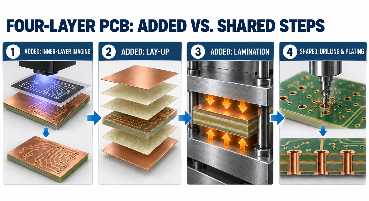
In a typical 4-layer build, the two inner copper patterns are formed on a core. Prepreg and outer copper foils are then arranged around that core and bonded under heat and pressure. Eurocircuits documents both inner-layer imaging and the multilayer lay-up and bonding process. Inner-layer imaging, alignment, lay-up, and lamination are the added multilayer operations; drilling and through-hole plating are also used on many 2-layer plated-through-hole boards. This guide to prepreg and core materials provides more detail on the multilayer construction. The additional materials and controlled operations explain why a 4-layer board generally has a higher fabrication cost than a comparable 2-layer board.
There is no reliable universal percentage. The layer count changes the process cost, while the board design determines how much material and manufacturing capacity each finished board consumes.
How Board Size and Panel Utilization Affect Cost
Larger boards generally cost more because fewer copies fit on a production panel. However, the relationship is not perfectly proportional to board area. The usable panel has fixed dimensions, process margins, and spacing between boards, so a small change in one board dimension can reduce the number of boards that fit across the panel. The cost can therefore move in steps. An unusually long, narrow, or irregular outline can also waste panel area even when its total area is not large. Eurocircuits explains that pooled circuits are priced partly by the panel area they occupy and their pooling efficiency.
Consider a simplified teaching example. Assume a usable panel area of 500 × 400 mm, ignore rails and spacing, and assume the same panel-processing cost for both designs. A 100 × 80 mm board fits 5 × 5, or 25 boards per panel. If a forced 2-layer layout increases the width to 120 mm, only 4 × 5, or 20 boards fit. The panel-related cost per board changes from one twenty-fifth of a panel to one twentieth—a 25% increase in this portion of cost, even though the board width increased by 20%. This is not a supplier quotation; real panel margins, rotation, defects, pooling, and order quantity change the result.
Making a board smaller usually improves material utilization, but it does not reduce price indefinitely. CAM preparation, tooling, setup, electrical testing, packaging, and minimum-order charges are partly fixed. Once those charges dominate, reducing a small board by a few millimeters may produce little or no quoted saving.
What Pushes a PCB Quote Up or Down
| Cost driver | Usually lowers cost | Usually raises cost | Why it matters when comparing 2 and 4 layers |
| Board outline and panel fit | Smaller rectangular outline that nests efficiently | Larger or awkward outline; a dimension that reduces boards per panel | A 2-layer design that needs more area can consume enough extra panel space to offset part of its layer-count saving |
| Order quantity | More boards per setup and efficient full-panel multiples often lower unit cost | Very small orders leave setup and engineering cost spread over few boards | Compare the same quantity; prototype promotions can hide the production-volume relationship |
| Stackup, material, and thickness | Standard FR-4 construction and a fabricator’s stocked thickness | Special laminate, nonstandard thickness, or a custom stackup | A standard 4-layer build may be more economical than a nonstandard 2-layer construction, although it still has more process steps |
| Copper weight | Standard copper for the selected service | Thicker copper, especially when it changes etching or lamination requirements | High-current requirements can raise either option’s cost; layer count alone does not identify the cheaper current-carrying solution |
| Trace, spacing, and hole rules | Relaxed dimensions within the standard process class | Finer traces and gaps, smaller drills, tighter annular rings, or higher drill aspect ratio | Forcing dense routing onto two layers may move the design into a more expensive technology class; Eurocircuits ties its pattern and drill classes to manufacturability and pricing |
| Surface finish and options | The supplier’s standard finish and solder-mask options | ENIG, hard gold, special masks, or other extra processes when the application requires them | Hold these surface-finish options constant; otherwise the quote is measuring more than the difference between two and four layers |
| Controlled impedance and testing | No impedance requirement where the interface does not need it | Controlled dielectric construction, tighter tolerance, coupons, and TDR verification | Four layers often provide easier geometry, but impedance coupons and verification can still add process control, panel area, and test work |
| Lead time and production route | Standard lead time, stocked stackup, and a poolable design | Rush service, nonstandard construction, or a design that cannot use the normal pooled process | Quote both versions at the same time and lead time; otherwise capacity and service-level differences can dominate the comparison |
The fairest comparison holds quantity, material family, finished thickness, copper weight, surface finish, electrical test, quality requirements, and lead time constant. Then quote the actual outline and stackup of each manufacturable design. Do not compare a compact 4-layer board with an imaginary 2-layer version of the same size if the 2-layer routing would actually require a larger board or tighter design rules.
Finally, separate bare-board price from total project cost. If the 2-layer version needs more layout time, a larger enclosure, another EMC test cycle, or a redesign, its cheaper fabrication quote may not be the cheaper product decision. If both versions meet the requirements at the same outline with similar engineering effort, two layers will usually remain the economical choice. For a broader breakdown of the variables behind an actual quotation, see this PCB manufacturing cost guide.
A Five-Step Way to Choose
Start with the required board outline and critical interfaces, then test whether a two-layer layout can preserve routing and reference-plane quality before comparing total cost.
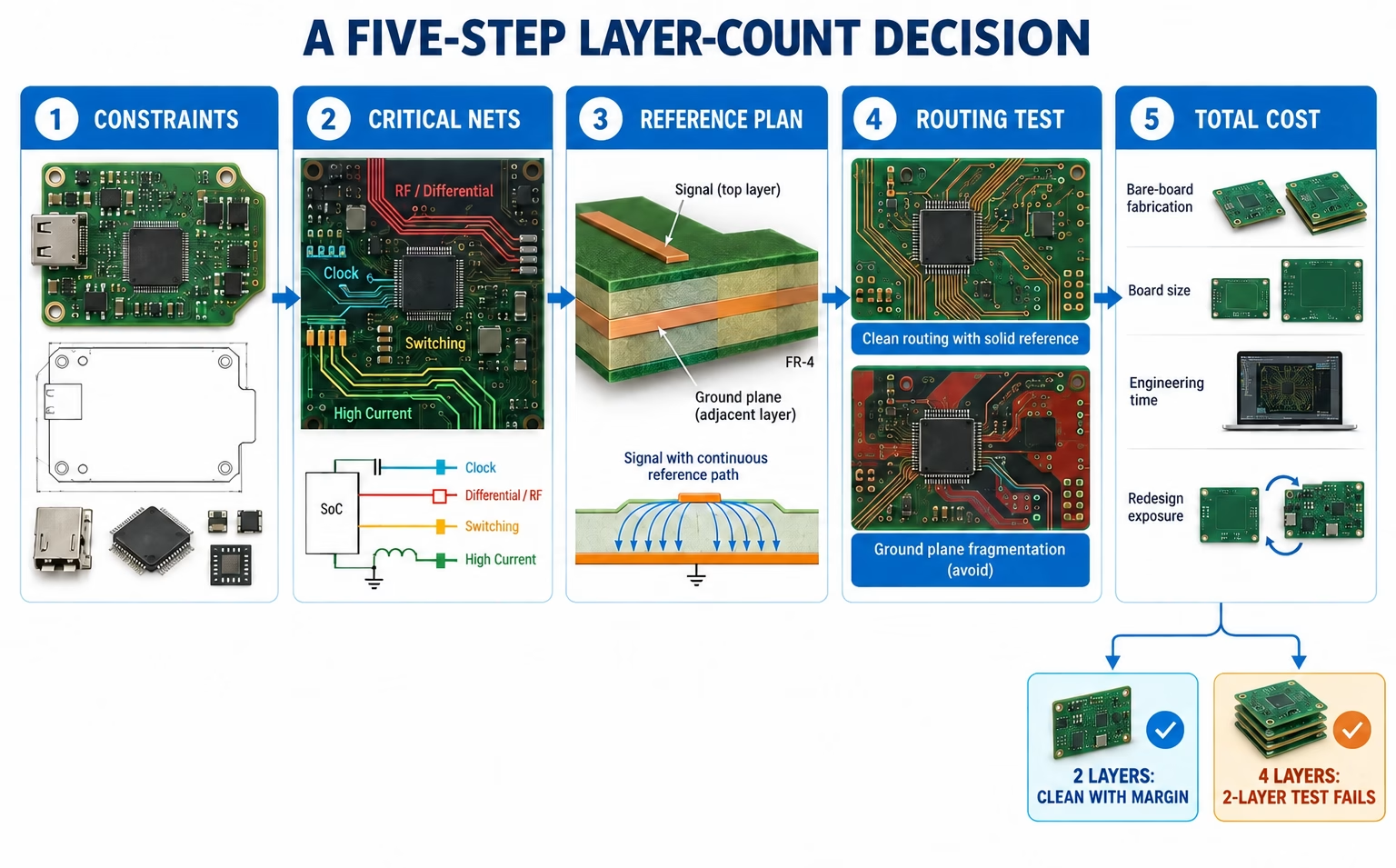
- Lock the non-negotiable constraints. Record the board outline, connector positions, component packages, power requirements, environmental limits, EMC target, and expected production volume.
- Identify the critical nets. Mark fast-edge signals, RF paths, clocks, differential interfaces, sensitive analog nodes, switching loops, and high-current paths. Use the relevant component or interface layout guides.
- Plan the reference and power structure. Decide where signal return currents will flow and how power will reach each load. Do this before filling both layers with ordinary routes.
- Test a realistic 2-layer placement and routing strategy. If it preserves ground continuity, meets spacing and width rules, and fits the required outline without heroic workarounds, keep two layers. If not, evaluate a 4-layer stackup early rather than forcing the layout.
- Compare total consequences. Quote the actual constructions, then consider layout time, board size, debug access, EMC margin, and the cost of a possible redesign. Choose the lower layer count only when it still satisfies the product requirements with reasonable margin.
Conclusion
Choose the lowest layer count that meets the layout and electrical requirements with reasonable margin—not simply the lowest bare-board price.
A spacious, carefully routed 2-layer PCB can be the better engineering choice for a simple design. A 4-layer PCB becomes worthwhile when it provides continuous references, routing room, predictable impedance, or a smaller outline that would be difficult to achieve on two layers. Evaluate the actual signal paths and stackup instead of relying on a component-count or frequency shortcut.
FAQ
Can a 2-layer PCB pass EMC testing?
Yes, a 2-layer PCB can pass EMC testing, but layer count alone cannot predict the result. Short switching loops, continuous return paths, good decoupling, filters, cables, and the enclosure all matter. Four layers often make return-path control easier; they do not guarantee compliance.
Is a 4-layer PCB always better than a 2-layer PCB?
No. Four layers provide more routing and reference-plane options, but a simple circuit may not benefit enough to justify the added fabrication complexity. A well-designed 2-layer board can be less expensive and easier to modify while still meeting all product requirements.
Can a 2-layer PCB use controlled impedance?
Yes. Controlled impedance is possible when the trace geometry, dielectric properties, board thickness, and reference plane are defined together. The required trace may become inconveniently wide on a thick 2-layer board, so verify the geometry against the fabricator’s stackup instead of assuming that two layers are unsuitable.
Can I convert a 2-layer PCB to four layers without changing the layout?
You can preserve much of the placement, but the design still needs an electrical review. Reassign ground and power, check which plane references each critical trace, recalculate controlled-impedance widths, and review layer transitions. Simply adding two internal copper layers may leave existing return-path problems unresolved.
Does a high-current PCB need four layers?
Not necessarily. Current capacity depends on copper thickness, conductor width and length, whether the copper is internal or external, allowable temperature rise, ambient conditions, and any vias in the current path. Extra layers can add parallel copper and spread heat, but the current path still needs to be sized with an applicable PCB-conductor method and verified for the actual construction by thermal analysis or measurement.
What is the most common 4-layer PCB stackup?
Signal–ground–power–signal is a common starting point. It is not universally best because bottom-layer signals may reference a split power plane. If both outer layers carry critical signals, a signal-plus-power/ground/ground/signal-plus-power arrangement may provide clearer return paths, provided power routing remains adequate.
Source
- UMEC — 2-Layer PCB vs 4-Layer PCB — used for competitor coverage of decision triggers and total project cost.
- Electrical Engineering Stack Exchange — 2-layer and 4-layer PCB stackup — used only for real-user questions about ground-plane assignment.
- Texas Instruments AN098 — Layout Review Techniques for Low Power RF Designs — used for conditional 2-layer and 4-layer RF stackup guidance.
- Texas Instruments — System Design Guidelines for the TM4C129x — used for device-specific stackup, interface, and 2-layer acceptance conditions.
- Texas Instruments — Practical PCB Design Rules — used for return-path discontinuity, loop area, and EMI explanation.
- Analog Devices — Basic Guidelines for Layout Design of Mixed-Signal PCBs — used for ground-plane and mixed-signal return-current guidance.
- Microchip — Two-layer Boards — used for 2-layer ground routing limitations and ground-grid guidance.
- Eurocircuits — Selecting the Right Surface Finish for Your PCB — used for finish process and relative cost direction.
- Sierra Circuits — 9 Cost Drivers for Rigid Circuit Boards — used for panel utilization and the added area and test work associated with controlled-impedance coupons.
- Analog Devices — Passing EMI Compliance Testing the First Time, Part 4 — used for the outer-signal/two-inner-ground 4-layer stackup option and stackup-planning context.

Get Quote Free