High-Speed PCB Design: Stackup, Impedance, and Routing Guide
A high-speed PCB is manufacturable when its stackup is built from the fabricator’s real dielectric data, impedance tolerance matches what the process can hold (typically ±8–10%, not ±5% everywhere), and routing rules sit inside the fab’s capability sheet. The gap between a board that simulates perfectly and one that returns at target impedance is the manufacturing handoff—not signal integrity theory.
Get Your PCB Quote!
Table of Contents
- 간략 사양: 고속 제조 설비 사양서에 담긴 실제 내용
- 스택업 핸드오프: 데이터시트 값이 아닌 실제 유전체 데이터
- 마이크로스트립 vs. 스트립라인: 임피던스 구조 선택
- 임피던스 허용 오차 사다리: 각 단계가 실제로 제공하는 이점은 무엇일까요?
- 임피던스 계산 방법 — 그리고 제작업체의 스택업 방식이 유리한 이유
- 제작 도면에서 제어 임피던스를 지정하는 방법
- 제조 현장에서 살아남는 라우팅 규칙
- 고속 DFM 검토: 거버 파일 전송 전 8가지 확인 사항
- FR-4와 고속 라미네이트: 업그레이드가 가치 있는 경우는 언제일까요?
- 고속 보드 가격을 실제로 좌우하는 요인은 무엇일까요?
- FAQ
- 고속 보드의 양산 가능성을 검토 중이신가요?
- 이 가이드에 대해
- 참고문헌 및 출처
- 관련 기사
Table of Contents
- 간략 사양: 고속 제조 설비 사양서에 담긴 실제 내용
- 스택업 핸드오프: 데이터시트 값이 아닌 실제 유전체 데이터
- 마이크로스트립 vs. 스트립라인: 임피던스 구조 선택
- 임피던스 허용 오차 사다리: 각 단계가 실제로 제공하는 이점은 무엇일까요?
- 임피던스 계산 방법 — 그리고 제작업체의 스택업 방식이 유리한 이유
- 제작 도면에서 제어 임피던스를 지정하는 방법
- 제조 현장에서 살아남는 라우팅 규칙
- 고속 DFM 검토: 거버 파일 전송 전 8가지 확인 사항
- FR-4와 고속 라미네이트: 업그레이드가 가치 있는 경우는 언제일까요?
- 고속 보드 가격을 실제로 좌우하는 요인은 무엇일까요?
- FAQ
- 고속 보드의 양산 가능성을 검토 중이신가요?
- 이 가이드에 대해
- 참고문헌 및 출처
- 관련 기사
A high-speed PCB design is manufacturable when its stackup is built from the fabricator’s real dielectric data, its impedance tolerance is set to what the process can hold (typically ±8–10%, not ±5% everywhere), and its routing rules sit inside the fab’s capability sheet — because a board that simulates perfectly in your layout tool and a board that comes back at 50Ω are separated by the manufacturing handoff, not by signal integrity theory.
📌Key Takeaways
- Impedance accuracy starts with the fabricator’s stackup, not your datasheet. Prepreg Dk varies with resin content, glass style, and press cycle; a nominal 4.2 FR-4 can measure anywhere in a 4.2–4.5 band.
- Industry-standard controlled-impedance tolerance is ±10%; a ±5% (or tighter) hold costs extra and buys real yield risk. Specify ±5% only on nets that genuinely need it.
- A 50Ω microstrip over 8 mil (0.20 mm) of FR-4 lands near 14 mil (0.36 mm) trace width — but the fabricator must recalculate with its real dielectric stack, which is why the worked example in this guide is marked (modeled).
- Microstrip is cheaper to build and easier to route; stripline gives better crosstalk isolation and a defined return path at higher layer and cost.
- The fab drawing should carry the stackup table, layer assignment, impedance net list, tolerance, and coupon requirement. Missing any one of these turns a routine order into a rework cycle.
Quick Specs: What a High-Speed Fab Capability Sheet Actually Says
At a glance: a fabricator that can build high-speed boards should state impedance tolerance, minimum trace geometry, aspect ratio, and test capability in writing — not in a sales conversation.
| Parameter | Value |
| Controlled impedance tolerance (standard) | ±8% (industry common: ±10%) |
| Controlled impedance tolerance (tight option) | ±5% |
| Minimum trace width / spacing | 1.8 mil (0.045 mm) |
| Layer count | 1–64 |
| Minimum mechanical drill | 0.1 mm |
| Minimum laser via | 3–6 mil |
| Drill aspect ratio (standard / advanced) | 12:1 / 16:1 |
| Impedance verification | Test coupons, flying probe, impedance test on every controlled lot |
| Governing design standards | IPC-2221C (design), IPC-2141A (controlled impedance), IPC-6012F (fab qualification) |
The numbers above are our own published capability sheet, and we treat capability claims from any other vendor the same way you should: verify them against the fab drawing before you design to them. The rest of this guide tells you what each row means for your design and how to check that the fabricator you picked can deliver it.
The Stackup Handoff: Real Dielectric Data, Not Datasheet Values
The single most common reason a controlled-impedance order comes back off-target is that the designer calculated trace widths with the laminate datasheet’s nominal Dk instead of the fabricator’s actual dielectric stack. FR-4’s datasheet says 4.2–4.5, but the number that matters is the effective Dk of your prepreg combination after lamination: resin content, glass style (106, 1080, 2116, 7628), and press cycle all move it.
When you send a high-speed design to a fab, you are not sending “impedance 50Ω.” You are sending a trace geometry over a dielectric thickness that the fabricator controls. The fab’s job is to pick prepreg and core combinations that hit your target width, spacing, and impedance together. That is why the correct flow is:
- Ask the fabricator for their preferred high-speed stackup (they will have two or three standard ones tuned to their material stock).
- Route to the widths and spacings that stackup produces for your targets.
- Confirm the stackup on the fab drawing before you release Gerbers.
What is the best 4-layer stackup for high-speed design?
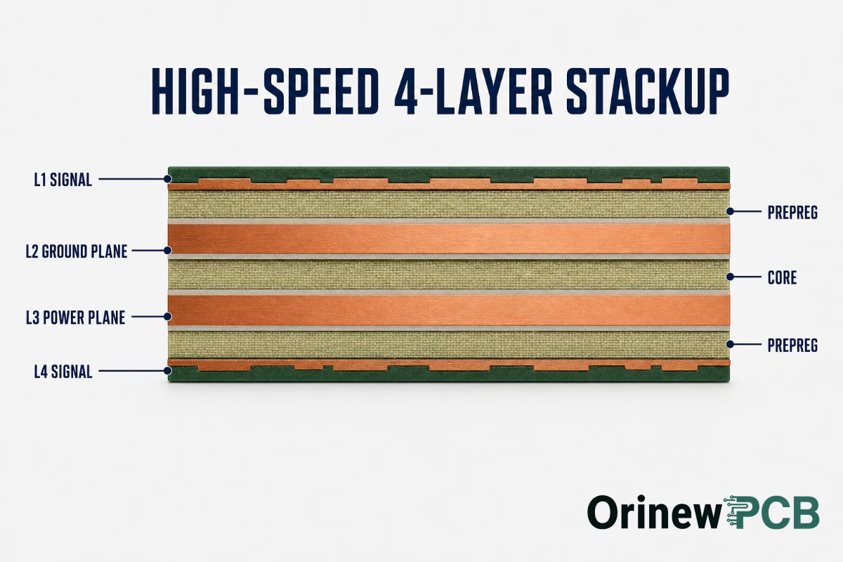
The best 4-layer stackup for a high-speed design is signal–ground–power–signal (L1 signal, L2 ground, L3 power, L4 signal), which puts every routing layer against a solid reference plane and gives both power and ground their own layers.
The alternative arrangement, signal–power–ground–signal, is workable when L3 is a dedicated ground and L2 is used for power routing only, but it forces the L3 ground to be broken for vias and often raises noise.
The standard 4-layer stackup in production is 1.6 mm (0.062 in.) total: ~8 mil (0.20 mm) core between L2–L3, ~5 mil (0.13 mm) prepreg between L1–L2 and L3–L4, and 1 oz (35 µm) copper. Note that the two signal layers sit as microstrip (L1, L4), so both routing layers reference an adjacent plane — that is the arrangement that makes controlled impedance achievable on four layers.
The 4-Layer Stackup Crosswalk
| Arrangement | Reference planes | What it gives you | Best for | Watch out for |
| SIG–GND–PWR–SIG | L2 ground, L3 power | Every signal layer against a solid plane; clean return paths | Most high-speed digital designs | L3 power plane must be split carefully if multiple voltages live on it |
| SIG–PWR–GND–SIG | L2 power, L3 ground | Power plane near top for decoupling reach | Designs with a few high-current rails | Ground (L3) gets broken by via fields; keep vias out of critical areas |
| SIG–GND–GND–SIG | Both inner layers ground | Maximum shielding, cheapest | Low-cost 4-layer boards with modest speeds | No dedicated power plane; route power as thick traces on signal layers |
| SIG–SIG–GND–GND | Two signal layers stacked | None for high-speed | Do not use for high-speed | Adjacent signal layers with no plane between them = crosstalk and no return path |
Decision rule: for a high-speed 4-layer board, start with SIG–GND–PWR–SIG, route both outer layers against their adjacent planes, and confirm the prepreg thicknesses with the fabricator before locking widths.
Microstrip vs. Stripline: The Impedance Structure Decision
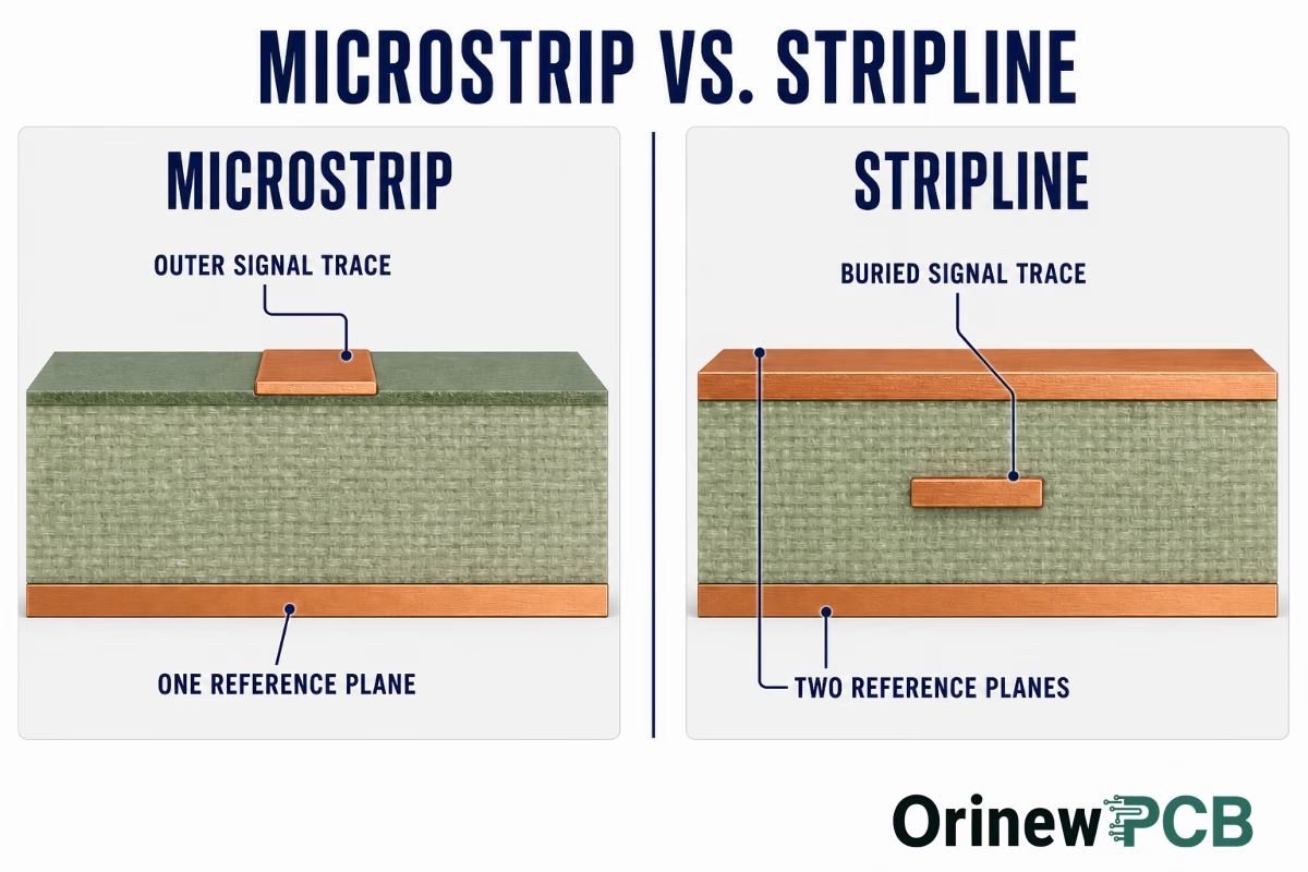
Microstrip wins on cost and routing freedom; stripline wins on isolation and a defined return path. The structure you choose decides where the signal layer sits, what reference it has, and what your impedance math looks like.
| Dimension | Microstrip | Stripline |
| Signal layer location | Outer layer (L1 or L4) | Buried between two planes |
| Reference plane | One adjacent plane | Two planes (above and below) |
| Crosstalk isolation | Moderate — signals exposed to each other and to the environment | Good — shielded on both sides |
| Impedance sensitivity | More sensitive to solder mask and surface finish over the trace | Less sensitive to mask; driven by core/prepreg thickness |
| Routing access | Easy — vias can drop straight to inner layers | Harder — signals are trapped between planes |
| Manufacturing cost | Lower — no extra layer count needed | Higher — needs at least two extra plane layers around it |
| Typical use | Single-ended clocks, shorter runs, outer-layer escape | Differential pairs, long high-speed lanes, EMI-sensitive nets |
Decision rule: route the critical differential lanes (USB, PCIe, Ethernet) as stripline when the layer budget allows it, and accept microstrip for single-ended signals and short runs where the cost of two extra layers is not justified. If you are on a 4-layer board, everything is microstrip by necessity — the decision only appears at six layers and up.
The Impedance Tolerance Ladder: What Each Rung Actually Buys You
Impedance tolerance is a cost and yield decision, not a signal quality badge. Moving from ±10% to ±5% roughly doubles the amount of re-engineering and test work a fab does, and that cost lands on your quote.
Industry-standard controlled-impedance manufacturing delivers ±10% tolerance.
A ±5% option is available from most capable fabs, and ±3% exists at boutique shops.
Our own standard process holds ±8%, with a ±5% tight option — which we quote deliberately, because not every net needs it.
The Impedance Tolerance Ladder
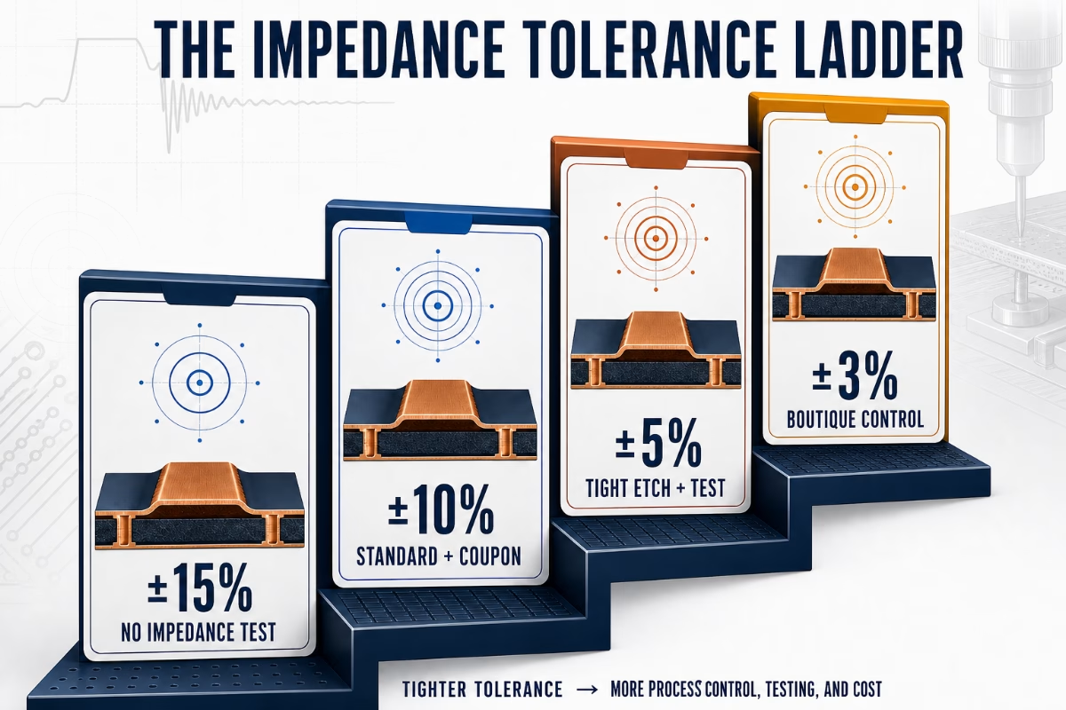
| Rung | Tolerance | What it means on the floor | When to use it | What it costs |
| Rung 1 | ±15% | Trace geometry roughly on target; no impedance test | Legacy designs, low-speed digital, no impedance requirement | Nothing extra |
| Rung 2 | ±10% | Standard controlled impedance with coupon verification | 50Ω single-ended, 90–100Ω differential at moderate speeds | Baseline |
| Rung 3 | ±5% | Tighter etch and dielectric control; more coupons, more test time | High-speed serial links, tight timing margins, RF input stages | Adds process + test premium |
| Rung 4 | ±3% | Boutique tolerance; limited material sets, longer lead times | Very high-speed links or RF where the design genuinely cannot absorb 5% | Significant premium, longer lead |
A common mistake is specifying ±5% for the entire board because one net is critical. The etch capability that delivers ±5% on the critical net is the same etch capability across the whole panel — but the coupon count, test time, and scrap risk are charged across the board. Scope the tolerance to the nets, not the order.
Decision rule: set the critical serial lanes to ±5% (or whatever your link budget demands), set everything else to the standard tolerance, and put the tolerance per net on the fab drawing rather than one blanket value.
How tight does differential-pair length matching need to be?
For a differential pair, keep the two legs matched within roughly 5 mil (0.13 mm) for most high-speed interfaces, and within 2–3 mil for very tight interfaces such as PCIe. In practice, community and vendor guidance converge on 5 mil as the working allowance for most designs — the mismatch converts to skew, and 5 mil of trace length is about 0.3 ps of propagation delay, which most link budgets absorb without difficulty. What matters more than the exact number is that length matching is done inside the pair (leg-to-leg) and that the pair’s total length stays within the interface’s budget (TI’s high-speed layout guidance, for example, notes that the etch lengths of USB 3.0 TX and RX groups do not need to match each other). Group-to-group matching is where designers overspend time for no measurable gain.
How to Calculate Impedance — and Why the Fabricator’s Stackup Wins
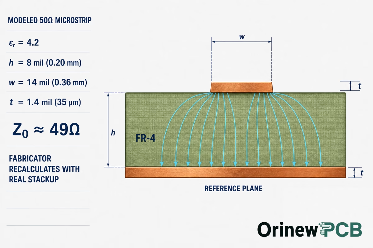
You can calculate a useful starting width for a 50Ω microstrip in about a minute; the fabricator then recalculates it against its real dielectric stack before the order runs. Both numbers matter: yours for routing feasibility, theirs for the actual etch.
The IPC-2141A microstrip approximation:
Z0 ≈ 87 / √(εr + 1.41) × ln(5.98h / (0.8w + t))
Where εr is the dielectric constant, h the dielectric height, w the trace width, and t the copper thickness.
Take standard FR-4 with εr = 4.2, an 8 mil (0.20 mm) dielectric height, and 1 oz copper (35 µm, about 1.4 mil):
Z0 = 87 / √(4.2 + 1.41) × ln(5.98 × 8 / (0.8 × 14 + 1.4))
Z0 = 87 / √5.61 × ln(47.84 / 12.6)
Z0 = 36.7 × ln(3.80) ≈ 36.7 × 1.33 ≈ 49 Ω
So a 14 mil (0.36 mm) trace over 8 mil of FR-4 lands close to 50Ω. This is a (modeled) starting point: the fabricator’s real prepreg combination will shift εr, and solder mask over the trace pulls microstrip impedance down 2–4 Ω, so the shipped width will differ by a mil or two. The point of the exercise is feasibility, not a final number.
For differential pairs, the common path is to start from the single-ended geometry and widen the spacing to lower the differential impedance toward target (90Ω for USB, 100Ω for Ethernet and most PCIe, 85Ω for some PCIe variants). The exact coupling depends on edge-to-edge spacing, which is why the fab’s impedance calculator, run on their stackup, is the number that goes on the drawing.
Decision rule: calculate your starting geometry in the layout tool, send the fabricator your target impedance per net, and let them return the stackup-adjusted width and spacing for sign-off. A fabricator that refuses to publish its impedance calculator or its standard stackups is a fabricator you will fight with on every revision.
How to Specify Controlled Impedance on the Fab Drawing
Controlled impedance is a five-part specification: stackup table, layer assignment, net list, tolerance, and coupon requirement. Missing any one part is how a “controlled impedance” order ships as a standard order.
The fab drawing is the contract. When it says “controlled impedance, 50Ω” without structure, the fab must guess — and guessing means the order gets built to the cheapest interpretation. What a complete specification looks like:
| Spec item | What to write | Why it matters | Limitation (not a guarantee) |
| Stackup table | Layer-by-layer: material, thickness, copper weight, prepreg style | Fixes the dielectric heights that impedance depends on | Only as good as the material stock on the day; confirm at quote |
| Impedance layers | Which layers carry controlled nets (e.g., L1, L4 microstrip) | Tells the fab where to apply tight etch control | Other layers still get standard etch |
| Net list | Target impedance per net: 50Ω single-ended, 100Ω differential, etc. | The fab’s calculator tunes width/spacing per net | Tolerances per net, not one blanket value |
| Tolerance | ±10%, ±8%, or ±5% per net group | Sets test scope and scrap risk | Tighter tolerance does not fix a marginal stackup |
| Coupon requirement | Impedance test coupon on the panel, verified by TDR | The only objective evidence the impedance was measured | Coupon matches the stackup, not every trace on the board |
| Finish note | Surface finish on impedance layers (e.g., ENIG over the microstrip) | Solder mask and finish shift microstrip impedance | Fab should report the as-built value, not the target |
A fabricator that builds high-speed boards daily will convert this specification into a standard impedance report with measured values per coupon. If the drawing is silent on any row above, the order is running on goodwill.
Decision rule: paste this table into your fab drawing template, fill every row before release, and ask for the impedance test report with the boards — not as a separate request after the fact.
Routing Rules That Survive the Fab Floor
Most routing rules for high-speed boards exist to protect signal integrity; the ones in this section exist because they are also manufacturable, and because ignoring them turns a good design into a rework loop.
| Rule | The signal-integrity reason | The manufacturing reason | What it means for your build |
| Solid reference plane under every critical trace | Return current follows the trace; a broken plane forces detours | Plane gaps under traces are invisible to etch but fatal to impedance | Route critical nets over solid planes; move via fields out from under them |
| Differential pairs: constant spacing, matched legs | Keeps differential impedance constant along the run | Uneven spacing reads as an etch or coupon anomaly | Keep pair spacing uniform; do the leg matching with gentle serpentines, not right angles |
| No right-angle turns on impedance traces | Corners create capacitance discontinuities | Right angles are an etch and solder-mask artifact risk at fine geometry | Use 45° chamfers or arcs; the fab can hold them at any geometry you can route |
| Via count and size matched to aspect ratio | Vias add stub and discontinuity | Aspect ratio above 12:1 needs sequential lamination or back-drilling | Confirm via aspect ratio against the capability sheet before finalizing stackup |
| 3W spacing on adjacent parallel traces | Reduces crosstalk between neighbors | Widely spaced traces are easier to etch and inspect | 3W is a practice, not a standard — adjust to your noise budget |
| No via-in-pad on impedance nets unless specified | Via-in-pad changes the pad’s impedance signature | Via-in-pad needs via-fill plating; adds cost and a failure mode | Use via-in-pad only when the pitch forces it, and tell the fab |
| Back-drilling for high-speed through-vias | Removes the unused via stub that reflects at high frequencies | Back-drilling is a separate process step with its own depth tolerance | Specify stub length or “back-drill to Lx”; expect a small cost add |
A mistake we see repeatedly in DFM review is a design that routes beautifully against the signal-integrity theory but violates the fab’s capability sheet somewhere invisible: an aspect ratio the drill can’t plate reliably, a via field that punches through a reference plane under a critical pair, or a differential pair that changes spacing at every bend. Those are the defects that show up as “intermittent” failures in the field, not at AOI.
Decision rule: before you finalize the layout, pull the fab’s capability sheet and check three numbers against it — trace width/space, drill aspect ratio, and via-in-pad support. If the sheet is not published, ask for it in the first email; it is the cheapest design review you will ever run.
The High-Speed DFM Review: 8 Checks Before You Send Gerbers
Eight checks reduce, not eliminate, the risk of a high-speed board coming back off-target. We run this review on every controlled-impedance order that passes through our DFM desk, and it is the same list you can run yourself before release.
The 8-Point High-Speed DFM Review — our own framework, not an industry standard.
| # | Check | Red flag | Limitation (not a guarantee) |
| 1 | Stackup uses fabricator’s dielectric data | Widths calculated from datasheet Dk, not the fab’s stackup | The fab’s stackup changes if material stock changes |
| 2 | Impedance layers and nets listed on the drawing | “Controlled impedance” with no net list or tolerance | The fab can only control what is written down |
| 3 | Tolerance scoped per net, not blanket | ±5% across the whole board because one net is critical | Tight tolerance on an unverified stackup still fails |
| 4 | Aspect ratio within capability | Through-via aspect ratio above the fab’s plated limit | Back-drilling or sequential lamination needed instead |
| 5 | Reference planes solid under critical traces | Via fields or splits under differential pairs | Plane gaps are the top field-failure cause we see |
| 6 | Differential pairs uniform and matched | Legs diverge at bends; spacing changes per segment | 5 mil leg matching is a working allowance, not a spec |
| 7 | Coupon requested and test method named | No coupon requirement on the drawing | Coupons verify the stackup, not every trace |
| 8 | Surface finish compatible with impedance layers | Finish change after the stackup was tuned | Mask and finish shifts microstrip by 2–4 Ω |
On a recent 6-layer HDI order through our review, the incoming DFM check caught a via field that punched through the L3 ground reference directly under a 100Ω pair — the design passed the layout tool’s DRC, and it would have passed electrical test, but the impedance coupon would have shown it and the pair would have been marginal in the field. The fix was moving the via field 2 mm, which cost nothing at the design stage and would have cost a re-spin at production. (Factory verification pending: confirm order details and numbers before publication.)
Decision rule: run the eight checks in order, and treat any red flag as a release blocker — not a “the fab will sort it out” item. A DFM review that finds nothing is a review that was not looking hard enough.
FR-4 vs. High-Speed Laminates: When the Upgrade Is Worth It
Standard FR-4 carries most high-speed designs to roughly 5–10 Gbps; beyond that, or when loss and skew matter, a low-loss laminate is the difference between a design that works and one that ships with its margin already spent.
| Dimension | Standard FR-4 | High-speed FR-4 (low-loss) | Rogers / PTFE-class |
| Dielectric constant (Dk) | ~4.2–4.5 (varies with resin) | ~3.8–4.2 (tighter spec) | 3.0–3.5 (stable across frequency) |
| Dissipation factor (Df) | ~0.020 | ~0.010–0.014 | 0.001–0.004 |
| Loss at high frequency | High — loss grows with frequency | Moderate | Low — stable to mmWave |
| Dk stability vs. frequency | Drifts | Moderate | Very stable |
| Cost | Baseline | +15–30% material premium | Several times FR-4 |
| Typical use | Most boards, <10 Gbps links | 10–25 Gbps server and switch designs | RF, radar, mmWave, very long high-speed lanes |
The decision rule of thumb used in practice: if your serial link is under ~10 Gbps and your trace runs are short, standard FR-4 with a well-controlled stackup is usually enough — the fab’s prepreg control matters more than the laminate grade. If the design runs 25 Gbps+, long reaches, or tight timing margins, the low-loss upgrade is cheap insurance compared with a field failure.
Decision rule: specify the laminate by Df and Dk stability, not by brand, and ask the fabricator which of its material stock holds the Df you need at your frequency. A datasheet Df measured at 1 MHz tells you nothing about loss at 10 GHz.
What Actually Drives High-Speed Board Cost
The cost drivers on a high-speed board are layer count, impedance tolerance scope, via processing, and material grade — in that order. The trace width and spacing that look exotic in the layout tool are usually the cheapest part of the order.
| Cost line | What it covers | Cost lever | 5-year view (modeled) |
| Layer count | More layers = more lamination cycles, more yield exposure | Every two layers beyond 4 roughly steps the price band | Adds cost every time the board is built — a permanent commitment |
| Impedance tolerance scope | Coupon count, test time, etch control | ±5% board-wide vs. per-net | Scrap and rework risk compound across every panel |
| Via processing | Back-drilling, via-fill, sequential lamination | Specify back-drill depth; avoid via-in-pad where possible | Saves a repeatable per-panel cost on every order |
| Material grade | FR-4 vs. low-loss vs. Rogers | Match Df to the actual link speed | A 15–30% material premium that buys margin, not decoration |
| Surface finish | ENIG, OSP, immersion finishes | Finish choice shifts impedance slightly and drives assembly yield | Pick at quote; changing mid-program adds re-verification |
Decision rule: get the cost conversation in the right order — lock the layer count and via processing first, then tolerance scope, then material. That ordering is what separates a realistic high-speed quote from a sticker-shock one.
FAQ
What tolerance can a fabricator actually hold on controlled impedance?
Standard controlled impedance is delivered at ±10% by the industry, and capable fabs offer ±5% (some ±3%) as a quoted option. Our standard process holds ±8%, with a ±5% tight option for critical nets. Tolerance is a yield and cost decision: scope it per net, not across the board.
Do I need to calculate impedance myself, or does the fabricator do it?
Both. You calculate a starting geometry to confirm routing feasibility; the fabricator recalculates against its real dielectric stack and returns the shipped width and spacing. The number on the fab drawing is the fabricator’s, verified by coupon.
What is the difference between a microstrip and a stripline for impedance?
Microstrip routes on an outer layer against one reference plane — cheaper, easier to route, more exposed to crosstalk. Stripline is buried between two planes — better isolation and a defined return path, at the cost of extra layers. Use stripline for critical differential lanes when the layer budget allows.
How much does a ±5% impedance tolerance add to the cost?
Expect a process and test premium on the order, and more scrap risk on tight panels. The practical lever is scoping ±5% to the critical nets instead of the whole board, which keeps the coupon and test cost focused where it matters.
When is a low-loss laminate actually worth the upgrade?
When the serial link runs at roughly 10–25 Gbps, the reach is long, or timing margin is tight. Below that, standard FR-4 with a well-controlled stackup and real prepreg control is usually sufficient — the laminate grade is the last lever, not the first.
Scoping a high-speed board for production?
Send us your layer count, target impedance per net, and expected signal speeds, and we will return a stackup recommendation, impedance-adjusted trace geometry, and a DFM review of your Gerbers — free, before you commit to production. You get back a documented stackup table and an impedance test plan, on a quote that names the tolerance per net.
Get a Free High-Speed DFM Review + Impedance Stackup →
About This Guide
This guide compiles published IPC design and qualification standards (IPC-2221C, IPC-2141A, IPC-6012F), manufacturer layout guidance, and our own fabrication and DFM experience on controlled-impedance boards. The worked impedance example is a modeled calculation to show feasibility, not a measured value — the shipped geometry is always the fabricator’s, verified by test coupon. Cost figures marked (modeled) are estimates calibrated against published industry ranges and our own quoting history, not forecasts. One first-party DFM anecdote is included with factory confirmation pending and is flagged for verification before publication. If you find a discrepancy with a current quote or a standard revision, tell us so we can correct this page.
References & Sources
- IPC-2221C, Generic Standard on Printed Board Design — Global Electronics Association (conductor spacing, design rules).
- IPC-2141A, Controlled Impedance Circuit Boards and High Speed Logic Design — Global Electronics Association (microstrip/stripline impedance design).
- IPC-6012F, Qualification and Performance Specification for Rigid Printed Boards — Global Electronics Association (fab qualification).
- IPC-A-610J, Acceptability of Electronic Assemblies — Global Electronics Association (assembly acceptance).
- High-Speed Layout Guidelines for Signal Conditioners and USB Hubs — Texas Instruments application note SLLA414 (differential-pair length matching; TX/RX group matching not required).
- PCB Impedance Control — industry tolerance norms: ±10% standard, ±5% option; vendor-reported.
- The Impact of PCB Manufacturing Tolerances on Impedance Control — tolerance impact on impedance; vendor-reported.
Related Articles
- PCB Impedance Control: What It Is and How to Calculate — the impedance basics and calculation methods this guide builds on.
- PCB Stackup Design Guide: Multilayer, 4-Layer & Flex — general stackup design decisions beyond high-speed.
- What is PCB Dielectric Constant (Dk)? — how Dk behaves across frequency and why it drives impedance.
- Master PCB Trace Width: Design, Calculate & Optimize — trace geometry and current capacity rules.
- PCB Material Selection: FR-4, Rogers, PTFE & Aluminum — the full material decision framework for any design.

Get Quote Free