Rogers RT/duroid 5870 Laminate: High-frequency PCB applications
Rogers RT/Duroid 5870 is a specialized microwave laminate designed for high frequency applications demanding tight electrical tolerances. This material is designed specifically for demanding stripline and microstrip circuit applications.
Get Your PCB Quote!
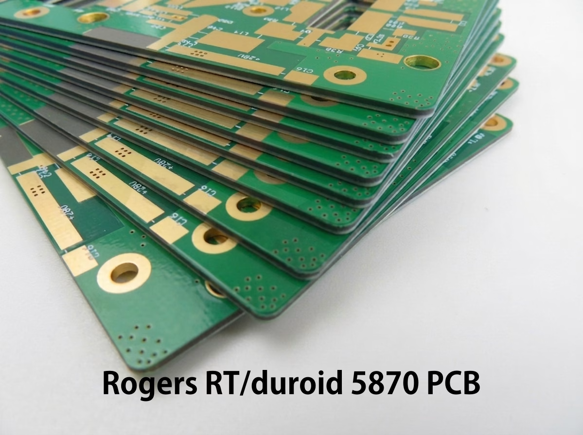
Table of Contents
Table of Contents
Microwave and millimeter-wave electronic systems demand substrate materials that manage high- frequency electromagnetic waves without causing excessive signal attenuation. Standard glass-epoxy materials introduce massive dielectric losses and phase distortions that degrade signal integrity above a few gigahertz. I once spent three weeks debugging a Ku-band radar prototype that failed field testing , only to realize standard FR-4 was introducing over 3 dB of unexpected signal attenuation.
Dielectric losses spike, impedance control breaks down, and your simulated design stops matching reality. Rogers RT/duroid 5870 was built to solve that problem.
Need PCB Manufacturing or Assembly?
Get a free quote within 24 hours. We specialize in prototype-to-production PCB/PCBA for hardware teams worldwide.
What is RT/Duroid 5870?
RT/Duroid 5870 is a glass microfiber reinforced PTFE (polytetrafluoroethylene) composite laminate manufactured by Rogers Corporation. Unlike woven glass, its randomly oriented microfibers create a uniform dielectric throughout the panel. This gives it isotropic electrical properties—signal velocity stays consistent in any direction.
The result: predictable, low-loss performance from a few GHz all the way into the millimeter-wave bands.
Electrical Properties
Key Specs at a Glance
| Property | Value | Test Condition |
| Dielectric Constant (Dk) | 2.33 ± 0.02 | 10 GHz, 23°C — IPC-TM-650 2.5.5.5 |
| Dissipation Factor (Df) | 0.0012 | 10 GHz, 23°C — IPC-TM-650 2.5.5.5 |
| TCDk (Temp. Coefficient) | −115 ppm/°C | Standard operating range |
What These Numbers Mean
The Dk of 2.33 is one of the lowest available for reinforced PTFE. A low Dk means wider trace widths for a given impedance—wider traces carry more RF power with lower resistive loss.
The Df of 0.0012 at 10 GHz is about 15–20× lower than FR-4. That gap translates directly into insertion loss. In a receiver chain, it is the difference between a useful signal and the noise floor.
The TCDk of −115 ppm/°C is predictable and linear. Engineers can compensate for it in phase-matched systems like phased-array radar. The dielectric constant also stays stable across a wide frequency range, so a wideband design (say, 2–18 GHz) will behave the same way at both ends of the band.
Mechanical & Thermal Properties
Thermal Specifications
| Property | Value | Test Method |
| CTE — X-axis | 22 ppm/°C | ASTM E831 |
| CTE — Y-axis | 28 ppm/°C | ASTM E831 |
| CTE — Z-axis | 173 ppm/°C | ASTM E831 |
| Thermal Conductivity | 0.22 W/m·K | ASTM C518 |
| Decomposition Temperature (Td) | >500°C | TGA |
| Moisture Absorption | 0.02% | IPC-TM-650 |
What to Watch
The Z-axis CTE of 173 ppm/°C is higher than copper. That matters for plated through-holes—plan for it during via design (see Section 5). The glass microfiber reinforcement controls in-plane expansion well, keeping X/Y CTE reasonable.
Moisture absorption below 0.02% is a key advantage over ceramic-filled alternatives. Absorbed moisture raises both Dk and Df, causing impedance drift. With RT/duroid 5870, performance stays stable in humid outdoor enclosures, on aircraft, and in space.
Decomposition above 500°C means the material is fully compatible with lead-free reflow soldering (260°C peak). Still, bake the board before reflow to drive off any ambient moisture.
Available Configurations
Standard Dielectric Thicknesses
| Thickness (in) | Thickness (mm) | Tolerance |
| 0.005″ | 0.127 | ± 0.0005″ |
| 0.010″ | 0.254 | ± 0.0007″ |
| 0.020″ | 0.508 | ± 0.0015″ |
| 0.031″ | 0.787 | ± 0.0020″ |
| 0.062″ | 1.575 | ± 0.0030″ |
Copper Cladding Options
- Electrodeposited (ED): 1/2 oz, 1 oz, 2 oz — standard option, good adhesion.
- Rolled Copper: 1/2 oz, 1 oz — smoother surface, lower conductor loss at higher frequencies.
- Reverse-Treated ED: Enhanced adhesion to PTFE with good RF performance.
For designs above 10 GHz, rolled copper or immersion silver/ENIG finishes will reduce conductor loss from the skin effect.
Design Guidelines
50Ω Microstrip Trace Widths
The low Dk of 2.33 requires wider traces than FR-4 for the same impedance. Use Rogers’ MWI-2017 calculator or an EM field solver—do not rely on generic PTFE assumptions.
| Substrate Thickness | Copper Weight | 50Ω Trace Width | Effective Dk |
| 5 mil (0.127 mm) | 0.5 oz (18 μm) | 14.2 mils (0.36 mm) | 1.82 |
| 10 mil (0.254 mm) | 1.0 oz (35 μm) | 28.5 mils (0.72 mm) | 1.85 |
| 20 mil (0.508 mm) | 1.0 oz (35 μm) | 58.1 mils (1.48 mm) | 1.88 |
| 31 mil (0.787 mm) | 1.0 oz (35 μm) | 91.2 mils (2.32 mm) | 1.91 |
Thicker substrates need wider traces. If routing is tight, switch to a thinner core (5 mil or 10 mil) to keep traces narrow. Coplanar waveguide (CPW) is another option—placing ground planes on the same layer as the signal trace keeps fields tighter and allows narrower lines on thick cores.
Impedance Control
RT/duroid 5870 offers ±0.02 Dk tolerance. That level of consistency makes tight impedance control realistic. For reference, FR-4 Dk can vary ±10%—on a narrow-band filter at 24 GHz, that variance alone can move your passband by hundreds of megahertz.
Use the Design Dk value of 2.33 in your simulator. Also account for the effective Dk (lower than bulk Dk) in microstrip, since fields exist partly in air above the trace.
Solder Mask and Surface Finish
Do not apply solder mask over RF traces. Standard LPI solder masks have high Df and will degrade signal quality above a few gigahertz. Keep RF lines bare or covered only with a low-loss surface finish.
Recommended finishes by application:
- ENIG— best solderability and corrosion resistance; slight increase in loss from the nickel layer.
- Immersion Silver — lowest insertion loss; may tarnish in harsh environments.
- HASL— acceptable up to ~10 GHz; rougher surface increases loss above that.
Via Design
The Z-axis CTE mismatch between PTFE (173 ppm/°C) and copper creates stress on plated through-holes during thermal cycling. To manage this:
- Keep via aspect ratios below 8:1.
- Use annular rings of at least 5 mils.
- Target copper plating thickness of 1.0–1.2 mils minimum.
- For high-reliability applications, use filled or capped vias.
Multilayer Stackups
A full RT/duroid 5870 multilayer build is expensive. A cost-effective alternative is a hybrid stackup: use RT/duroid 5870 only for outer RF layers, and FR-4 or high-Tg epoxy for inner layers. This keeps the RF path on low-loss material while FR-4 provides mechanical rigidity.
Standard FR-4 prepreg does not bond well to PTFE. Use Rogers RO4450F bondply or a thermoplastic FEP film for hybrid lamination. Keep the stackup symmetric to avoid warpage, and align grain directions between laminate sheets.
Fabrication Guidelines
PTFE is soft and chemically inert—both properties create challenges during fabrication. Standard FR-4 processes will not work without modification. Always use a fabricator with certified experience on PTFE-based materials.
Drilling
| Parameter | Specification |
| Drill type | Carbide, 130° included lip angle |
| Surface speed | 150–250 SFM (45–75 m/min) |
| Chip load | 0.001–0.002″ per revolution |
| Max stack height | 0.240″ (6.1 mm) |
| Entry/exit material | Pressed phenolic composite boards |
| Drill condition | New or precision-ground bits strongly recommended |
PTFE tends to smear into drilled holes. Plasma desmear or sodium treatment is mandatory before plating—never skip this step.
Chemical Surface Activation
PTFE is inert. Electroless copper will not adhere to untreated hole walls. You must chemically activate the surface first:
- Sodium-naphthalenate (wet) treatment: Removes fluorine atoms from the PTFE surface, creating reactive bonding sites. Products like Tetra-Etch are commonly used.
- Plasma treatment (dry): Uses H₂/N₂ or NH₃ gas to modify surface chemistry. Preferred for direct metallization processes.
After activation, deposit electroless copper, then electroplate to a target thickness of ~20 μm. Uniform plating thickness is critical—thin spots create stress concentration points during thermal cycling.
Etching
| Parameter | Specification |
| Compatible etchants | Ferric Chloride, Ammonium Persulfate, Cupric Chloride |
| Etch factor (1 oz copper) | 1.5–2.0 |
| Etch factor (2 oz copper) | 2.0–2.5 |
| Post-etch rinse | Thorough DI water rinse required |
Routing and Edge Quality
Use carbide routing bits at high feed rates with moderate spindle speeds. This prevents the bit from lifting the copper cladding away from the soft PTFE core. Clean board edges are especially important for edge-launch connectors, which must seat flush against the substrate.
Material Comparison
RT/duroid 5870 vs. RT/duroid 5880
| Property | RT/duroid 5870 | RT/duroid 5880 |
| Dielectric Constant (Dk) | 2.33 ± 0.02 | 2.20 ± 0.02 |
| Dissipation Factor (Df) | 0.0012 | 0.0009 |
| Frequency Stability | Excellent | Excellent |
| Relative Cost | Moderate | Higher |
| Best For | General RF/microwave up to Ku-band | Ultra-low-loss: satellite transponders, LNAs |
Choose 5870 for most radar, antenna, and communications applications. Choose 5880 when every fraction of a dB matters—such as in a low-noise amplifier front end or a satellite transponder where thermal noise budget is tight.
RT/duroid 5870 vs. FR-4
| Property | RT/duroid 5870 | Standard FR-4 |
| Dielectric Constant | 2.33 ± 0.02 | 4.2–4.8 ± 10% |
| Dissipation Factor @ 10 GHz | 0.0012 | 0.02–0.025 |
| Moisture Absorption | 0.02% | 0.1–0.3% |
| Dk Stability vs. Frequency | Excellent | Poor above 1 GHz |
| Max Practical Frequency | 40+ GHz | ~2 GHz |
| Cost (approx.) | $150–250/sq ft | ~$5–10/sq ft |
The cost premium is significant—but so is the performance gap. At 10 GHz, FR-4’s Df is roughly 15–20× higher. For anything above 1–2 GHz where loss matters, FR-4 is not a viable substrate.
Applications
| Application | Why RT/duroid 5870 | Typical Frequency |
| Military phased-array radar | Stable Dk across temp. extremes; thick copper for high peak-power pulses; low moisture absorption in marine/airborne use. | Ku, Ka, W band |
| Satellite communications (LNB, transponders) | Ultra-low Df minimizes noise in vacuum (no convection cooling); near-zero outgassing; isotropic for circular polarization. | Ka band and above |
| Aircraft broadband antennas | Moisture resistance prevents Dk shifts through altitude/humidity swings during flight. | Ku band |
| Point-to-point microwave backhaul | Broad frequency stability supports multi-Gb/s data rates; chemical resistance for outdoor tower installations. | 18–80 GHz |
| 5G mmWave base stations | Low loss at millimeter-wave bands enables acceptable link budgets at short cell ranges. | 28, 39 GHz |
| RF calibration standards & test fixtures | Tight ±0.02 Dk tolerance makes electrical properties traceable and repeatable. | DC to mm-wave |
| Microstrip filters, couplers, power dividers | Low Df and isotropic properties give good agreement between simulation and measurement. | 1–40 GHz |
Frequently Asked Questions
What is the maximum operating frequency?
RT/duroid 5870 is usable well into millimeter-wave bands. Rogers specifies it for applications above 40 GHz. Below 30 GHz, dielectric loss dominates. Above 30 GHz, conductor loss from the skin effect becomes increasingly significant—use rolled copper or smooth surface finishes (ENIG, immersion silver) at those frequencies.
Can I use it in a multilayer build?
Yes. Both fusion bonding (no adhesive, optimal electrical performance) and adhesive bonding (using RO4450F prepreg) are supported. Hybrid builds with FR-4 inner layers are also common to reduce cost. See Section 5 for stackup recommendations.
Can I hand-solder components?
Yes, but use a temperature-controlled iron and work quickly—complete each joint in under 3 seconds. Prolonged heat exposure can delaminate pads from the soft PTFE substrate.
Is it compatible with lead-free reflow?
Yes. The decomposition temperature exceeds 500°C, well above the 260°C peak for lead-free profiles. Pre-bake the boards to remove absorbed moisture before running the reflow oven.
Why is sodium-naphthalenate treatment required?
PTFE’s chemical structure is extremely inert. Without surface treatment, electroless copper will not bond to via hole walls. The sodium treatment removes fluorine atoms from the polymer surface, creating reactive sites for copper adhesion. Skipping this step causes via barrel failures and delamination.
How does it compare to ceramic substrates?
RT/duroid 5870 costs roughly 50% less than ceramic while offering comparable electrical performance. Ceramics offer slightly lower losses and better thermal conductivity, but they are brittle and harder to fabricate for complex geometries. RT/duroid 5870 can be drilled, routed, and machined with standard PCB equipment.
How to Order
Specify These Parameters
- Dielectric thickness and tolerance (see Section 4 table)
- Copper type: electrodeposited, rolled, or reverse-treated
- Copper weight: 1/2 oz, 1 oz, or 2 oz
- Panel size requirements (standard up to 24″ × 18″)
- Any special processing requirements
Lead Times and Pricing
| Item | Typical Value |
| Production lead time | 4–6 weeks through authorized distributors |
| Prototype availability | Often from stock |
| Cost | ~$150–250/sq ft (varies by thickness and configuration) |
Summary
Designing microwave and millimeter-wave electronic circuits requires a transition from standard FR-4 to high-performance fluoropolymer substrates like Rogers RT/duroid 5870. The combination of an ultra-low dielectric constant of 2.33 and an exceptional dissipation factor of 0.0012 makes this material the premier choice for minimizing signal attenuation and phase distortion. By understanding the specialized machining parameters, ensuring chemical surface activation for reliable via plating, and utilizing hybrid lamination techniques, engineers can confidently design high-reliability radar and satellite systems that perform predictably under extreme environmental conditions.

Get Quote Free