Rogers RO4360G2 PCB: High-Dk RF Laminate Guide
Rogers RO4360G2 delivers Dk 6.15, 0.80 W/m·K thermal conductivity, and FR-4-compatible processing—eliminating the via cracking and yield losses that plague high-Dk PTFE in multilayer RF boards.
Get Your PCB Quote!
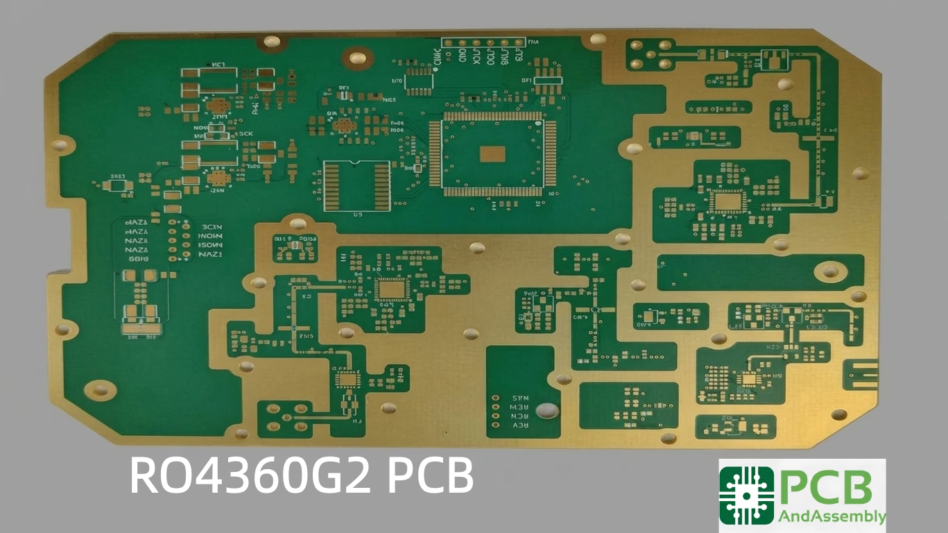
Table of Contents
If you’ve been searching for a high-Dk laminate that doesn’t require specialized PTFE processing, RO4360G2 PCB is probably on your shortlist. I’ve worked with this material on several RF designs over the past few years, and honestly, it fills a gap that many engineers didn’t realize existed until Rogers introduced it.
It is a high-Dk (6.15) thermoset laminate that behaves mechanically like FR-4 but performs electrically like a premium RF material. Unlike PTFE, which typically demands specialized sodium naphthenate or plasma etching for through-hole preparation, RO4360G2 integrates directly into standard PCB fabrication lines—without the yield-killing “special handling” fees that eat into your project budget.
What is RO4360G2 PCB Material?
RO4360G2 is a glass-reinforced, hydrocarbon ceramic-filled thermoset laminate from Rogers Corporation, belonging to the well-established RO4000 series. While the chemistry sounds complex, it is what defines the material’s practical utility. Most high-performance RF substrates are PTFE (Teflon) based—notoriously difficult to process because PTFE is a thermoplastic. It softens and moves when heated, creating dimensional instability that plagues multilayer builds.
RO4360G2 is a thermoset. Once cured, it stays rigid. Rogers engineered this material specifically to fill the gap for designers who need the miniaturization benefits of a high dielectric constant without the manufacturing overhead or mechanical instability associated with high-Dk PTFE laminates.
| Property | Value (Typical) | Test Method |
| Dielectric Constant (Dk) – Process | 6.15 ± 0.15 | IPC-TM-650 2.5.5.5 |
| Dielectric Constant (Dk) – Design | 6.40 | Differential Phase Length |
| Dissipation Factor (Df) @ 10 GHz | 0.0038 | IPC-TM-650 2.5.5.5 |
| Thermal Conductivity (W/m/K) | 0.80 | ASTM C518 |
| Glass Transition Temp (Tg) | >280°C | IPC-TM-650 2.4.24 (TMA) |
| Decomposition Temp (Td) | 390°C | TGA 5% weight loss |
| Z-Axis CTE | 28 ppm/°C (below Tg) | IPC-TM-650 2.4.41 |
| Moisture Absorption | 0.06% | IPC-TM-650 2.6.2 |
| Volume Resistivity | 1.7 × 10¹⁰ MΩ·cm | C-96/35/90 |
Table 1: Core Electrical and Thermal Specifications for RO4360G2
Need PCB Manufacturing or Assembly?
Get a free quote within 24 hours. We specialize in prototype-to-production PCB/PCBA for hardware teams worldwide.
Why Dk 6.15 Is the Sweet Spot for Miniaturization
In RF design, the physical size of distributed elements—patch antennas, filters, impedance-matching stubs—is inversely proportional to the square root of the dielectric constant. Moving from a standard RO4350B (Dk 3.48) to RO4360G2 (Dk 6.15) is not a marginal improvement. It fundamentally shortens the electromagnetic wavelength within the substrate, enabling real reductions in board real estate.
In practice, designers have achieved 20–30% area reductions on RF sub-circuits simply by migrating to this higher-Dk substrate. This matters most in Small Cell and Distributed Antenna System (DAS) deployments where enclosure dimensions are fixed and component density is continuously increasing.
There is a tradeoff worth acknowledging: higher Dk forces narrower trace widths for the same characteristic impedance. On thin laminates targeting a 50-ohm microstrip, traces may drop to 4–5 mils, requiring tighter etching tolerances. Confirming these dimensions with your fabricator’s DFM review before taping out is essential.
Important design note: always use the Design Dk of 6.4 in your simulation tools, not the process value of 6.15. Rogers publishes both values for good reason—designing to the process Dk will cause you to chase impedance mismatches during prototyping.
Thermal Performance in High-Power Applications
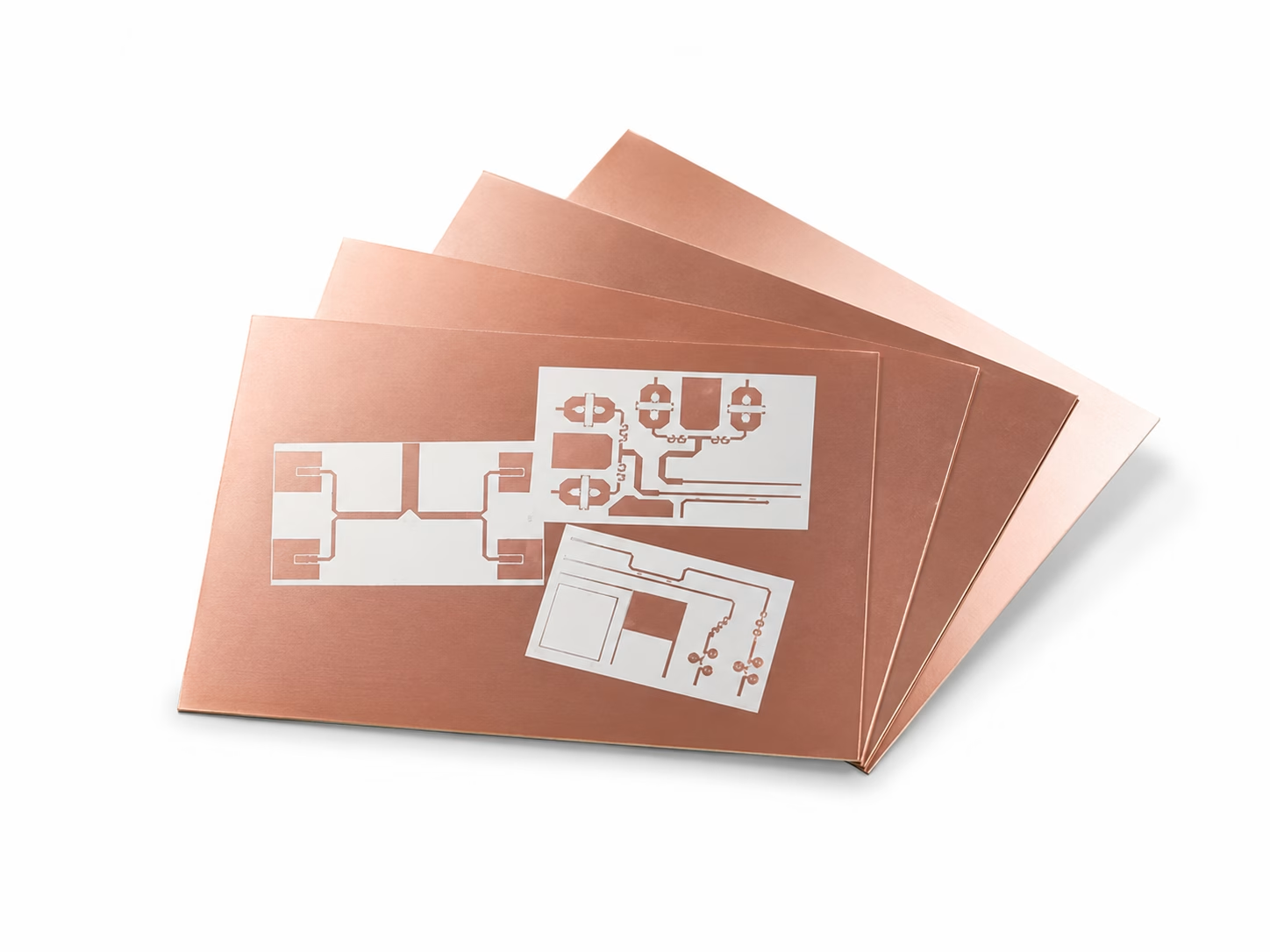
Heat is the primary failure mechanism in power amplifiers. RO4360G2 addresses this with a thermal conductivity of 0.80 W/m/K, roughly three times better than standard FR-4 (0.25 W/m/K). While it doesn’t match specialized thermally conductive laminates that can reach 1.0–1.5 W/m/K, it comfortably outperforms most PTFE-based alternatives in the 0.45–0.50 W/m/K range.
This thermal advantage allows heat generated by active components—GaN or LDMOS power transistors—to spread more efficiently through the dielectric into ground planes and ultimately the heat sink. For high-power designs, using 2 oz copper on internal layers further capitalizes on this thermal path. If the thermal load is extreme, RO4360G2 is also compatible with embedded copper coins and dense thermal via arrays.
| Material | Thermal Conductivity (W/m/K) | Max Continuous Temp | Primary Benefit |
| Standard FR-4 | 0.25 | 130–140°C | Low cost, low power |
| RO4360G2 | 0.80 | 150°C+ | High power density, compact size |
| RO4350B | 0.69 | 150°C+ | Industry-standard RF performance |
| PTFE (High-Dk) | 0.45–0.50 | 125°C | Lowest loss, mechanical risk |
Table 2: Thermal Management Comparison Across Common RF Laminates
Why Z-Axis CTE Kills Multilayer Boards—and How RO4360G2 Solves It
One of the most overlooked datasheet values is the Z-axis Coefficient of Thermal Expansion. When a PCB passes through a lead-free reflow oven peaking at 260°C, copper in the via barrels expands at roughly 17 ppm/°C. If the surrounding laminate expands at 100–200 ppm/°C as many high-Dk PTFE materials do, it applies immense tensile stress on the copper barrel. This eventually produces barrel cracking or corner cracking at the via/pad interface—failures that are often intermittent, hard to diagnose, and catastrophic at field deployment.
RO4360G2 has a Z-axis CTE of 28 ppm/°C (below Tg). This is dramatically lower than PTFE alternatives. The result is that the laminate and the copper via expand at much more compatible rates through the reflow cycle, protecting via integrity over hundreds of thermal cycles. We have observed PTFE-based boards showing via failures after just 5–10 thermal cycles under similar conditions; RO4360G2 boards in the same test regime routinely complete hundreds of cycles without via degradation.
This single characteristic—Z-axis CTE compatibility with copper—is arguably the primary reason RO4360G2 yields are so superior in 8-layer-and-above multilayer designs.
| Property | RO4360G2 | Typical High-Dk PTFE | High-Tg FR-4 |
| Z-Axis CTE (ppm/°C) | 50 (below Tg) | 100–200 | 45–60 |
| X/Y Axis CTE (ppm/°C) | 17 / 17 | 9–15 | 14–16 |
| Flexural Strength | 207 MPa | Low (1–2 kpsi) | High (60+ kpsi) |
| Tg (°C) | >280 | ~280 (varies) | 170–180 (high-Tg) |
| Specific Gravity | 2.2 | 2.1–2.5 | ~1.8 |
Table 3: Mechanical and Thermal Expansion Properties Comparison
Fabrication Reality: What FR-4-Like Processing Actually Means
When a materials supplier claims a substrate “processes like FR-4,” they are specifically referring to three operations: drilling, plated through-hole (PTH) preparation, and multi-stage lamination. These are the steps where PTFE-based boards diverge sharply from standard fabrication practices—and where costs and yield losses accumulate.
Drilling and Tool Wear
RO4360G2’s ceramic filler makes it abrasive. The same drill bit that handles 1,000 hits on an FR-4 panel will dull prematurely on RO4360G2. Best practice is to reduce the hit count per drill bit by 40–50% compared to FR-4 parameters. Clean hole walls are the foundation of reliable plating, and the extra tooling cost is trivial compared to the yield risk from rough vias.
No Plasma or Sodium Etch Required
PTFE requires a sodium etch or plasma etch to alter the via wall’s surface energy so that electroless copper will adhere. This is expensive, requires specialized chemistry, and many contract manufacturers either cannot perform it or charge a significant premium. RO4360G2 uses a standard desmear process—both CF₄/O₂ plasma and alkaline permanganate work well. If your fab house can build a high-reliability industrial board, they can build an RO4360G2 board.
Oxide Treatment and Lamination
Standard reduced oxide, brown oxide, or oxide alternative treatments are all compatible with RO4360G2. For lamination in multilayer builds, follow the processing guidelines for the RO4450F or RO4460G2 prepreg, which specify appropriate temperature ramps and pressure settings to achieve void-free bond lines.
Hybrid Stackups: Pairing RO4360G2 with RO4400 Series Prepreg
An 8-layer board made entirely of RO4360G2 core material is unnecessary and uneconomical. The practical approach is a hybrid stackup—using RO4360G2 for the critical RF signal layers (typically top and bottom microstrip layers) and lower-cost RO4400 series prepreg or compatible FR-4 for internal digital and power routing layers.
RO4450F and RO4460G2 prepregs are the engineered bonding agents for this approach. Their thermoset chemistry is formulated to be compatible with the RO4000 family, ensuring that peel strength remains high through multiple reflow cycles. Avoid mixing RO4360G2 with unqualified “high-Tg” FR-4 prepreg from arbitrary sources—CTE mismatch between dissimilar resin systems can cause warpage (“potato-chipping”) during cooling from lamination temperatures.
A representative 4-layer hybrid stackup:
| Layer | Material | Function | Thickness |
| L1 (Signal) | RO4360G2 | RF microstrip routing | 20 mil core |
| Prepreg | RO4450F | Bonding layer | ~4 mil |
| L2 (Ground) | Copper plane | RF ground reference | 1 oz |
| Core | RO4003C or RO4350B | Digital / power routing | 20 mil core |
| L3 (Power) | Copper plane | DC power distribution | 1 oz |
| Prepreg | RO4450F | Bonding layer | ~4 mil |
| L4 (Signal) | RO4360G2 | RF microstrip routing | 20 mil core |
Table 4: Example 4-Layer Hybrid Stackup Using RO4360G2 and RO4003C

About OrinewPCB
Time is money in your projects – and OrinewPCB gets it. OrinewPCB is a PCB assembly company that delivers fast, flawless results every time. Our comprehensive PCB assembly services include expert engineering support at every step, ensuring top quality in every board. As a leading PCB assembly manufacturer, we provide a one-stop solution that streamlines your supply chain. Partner with our advanced PCB prototype factory for quick turnarounds and superior results you can trust.
Primary Applications for RO4360G2
Base Station Power Amplifiers

Power amplifiers in 4G/5G base station infrastructure require substrates that maintain stable Dk under thermal stress while dissipating heat efficiently. RO4360G2’s combination of Dk stability, 0.80 W/m/K thermal conductivity, and lead-free process compatibility makes it a strong fit for PA designs in both macro and remote radio head (RRH) form factors.
Patch Antennas and Phased Arrays
The high Dk enables patch elements 25–30% smaller than those designed on Dk ~3.5 materials. In phased array and MIMO antenna panels where element spacing is a fixed fraction of wavelength, this reduction allows more elements per panel area or enables a given array to fit within a smaller enclosure.
Small Cell and DAS Transceivers

5G densification is driving demand for small cell nodes that are physically compact, thermally reliable, and cost-effective to manufacture at volume. RO4360G2 satisfies all three requirements and eliminates the fabrication complexity that would otherwise make PTFE-based high-Dk materials impractical for high-volume production.
Automotive Radar (ADAS)
Modern ADAS radar modules operate across extreme temperature ranges, from sub-zero winter conditions to underhood heat soaking. RO4360G2’s operating range of -55°C to +125°C, combined with its CAF resistance and low moisture absorption (0.06%), supports long-term reliability in demanding automotive environments.
Ground-Based and Airborne Radar
Radar systems demand consistency across temperature extremes and long operational lifetimes measured in decades. Low moisture absorption and stable Dk with temperature contribute to predictable performance over time, and FR-4-compatible processing reduces fabrication risk compared to PTFE-based alternatives.
Surface Finish Selection
The surface finish choice affects both RF performance (via skin-effect losses and surface roughness) and assembly reliability. For most RF applications, the recommendation is Immersion Silver (ImAg), which offers the lowest loss and excellent solderability. ENIG is the right choice when wire bonding or multiple reflow cycles are required.
| Surface Finish | RF Performance | Assembly Compatibility | Relative Cost |
| Immersion Silver (ImAg) | Excellent | Good (limited shelf life) | Moderate |
| ENIG | Good | Excellent (multiple reflows) | Higher |
| Immersion Tin | Good | Good | Lower |
| OSP | Good | Limited shelf life | Lowest |
| HASL (Lead-free) | Moderate | Excellent | Lower |
Table 5: Surface Finish Options for RO4360G2 RF Applications
RO4360G2 vs. RO4350B vs. PTFE
Laminate selection is always a set of tradeoffs. If minimizing signal loss is the only priority, a pure PTFE substrate like RT/duroid is technically superior. If cost is the only constraint, FR-4 wins. RO4360G2 is the engineering compromise that makes commercial RF products manufacturable.
| Priority | RO4360G2 | RO4350B | High-Dk PTFE |
| Smallest footprint (High Dk) | Best (Dk 6.15) | Not suitable (Dk 3.48) | Depends on grade |
| Lowest signal loss | Good (Df 0.0038) | Excellent (Df 0.0037) | Best |
| Multilayer via reliability | Best-in-class | Excellent | High risk |
| Heat dissipation | Excellent (0.80 W/m·K) | Good (0.69 W/m·K) | Poor (0.45–0.50) |
| Fabrication simplicity | FR-4 compatible | FR-4 compatible | Requires special processing |
| Volume production cost | Medium | Medium-low | High |
Table 6: Decision Matrix — When to Choose RO4360G2, RO4350B, or PTFE
Useful Resources for RO4360G2 PCB Design
Here are the essential documents and tools for working with RO4360G2:
Official Rogers Documentation
- RO4360G2 Data Sheet– Complete specifications and typical properties
Download: rogerscorp.com/ro4360g2-data-sheet
- RO4360G2 Processing Guidelines– Fabrication recommendations
Available from Rogers technical support
- RO4400 Bondply Data Sheet– Prepreg specifications for multilayer builds
Download from Rogers Advanced Electronics Solutions portal
Design Tools
- Rogers MWI Calculator– Microstrip and stripline impedance calculator
Access: pcbandassembly.com/impedance-calculator/
- Laminate Properties Tool– Compare materials and filter by parameters
Access: Rogers ACS website
Frequently Asked Questions
Does RO4360G2 require special storage?
No. The material has a long shelf life and a low moisture absorption rate of 0.06%, making it considerably more robust than older generations of ceramic-filled laminates. Standard PCB material storage conditions apply.
Is RO4360G2 RoHS and WEEE compliant?
Yes. It is fully lead-free process capable, surviving peak reflow temperatures to 260°C without degradation, and meets all applicable RoHS and WEEE environmental directives.
Can I use RO4360G2 for 5G mmWave designs?
For sub-6 GHz 5G applications, RO4360G2 is an excellent choice for miniaturization. For mmWave designs above 30 GHz, most engineers prefer lower-Dk materials to keep trace widths manageable and reduce dielectric losses at those frequencies.
What copper weights are available?
RO4360G2 is available with ½ oz, 1 oz, and 2 oz copper cladding across all standard dielectric thicknesses (8 mil to 60 mil). For power amplifier applications, 2 oz copper on inner layers improves both thermal dissipation and conductor loss.
What surface finish delivers the best RF performance?
Immersion Silver (ImAg) is generally preferred for lowest RF loss, as it avoids the skin-effect losses that nickel introduces in ENIG at high frequencies. For designs requiring wire bonding or multiple reflow exposures, ENIG is the more reliable choice despite slightly higher insertion loss.
Summary
Rogers RO4360G2 is a high-dielectric constant thermoset laminate that bridges the gap between high- frequency performance and manufacturing practicality. With a Dk of 6.15 and a design Dk of 6. 4, it enables significant circuit miniaturization. Its Z-axis CTE of 28 ppm/°C and high thermal conductivity of 0 .75 W/m/K make it particularly well-suited for high-power, high-reliability multilayer RF boards like power amplifiers and small cell base stations. Because it processes similarly to FR-4, it avoids the high costs and low yields associated with PTFE-based high-Dk alternatives.
Get Quote Free