Top 11 Ceramic PCB Manufacturers: Match the Process to Your Design
Compare 11 ceramic PCB manufacturers by DBC, AMB, thin-film and thick-film capabilities. Match substrate, circuit and assembly scope to your design.
Get Your PCB Quote!
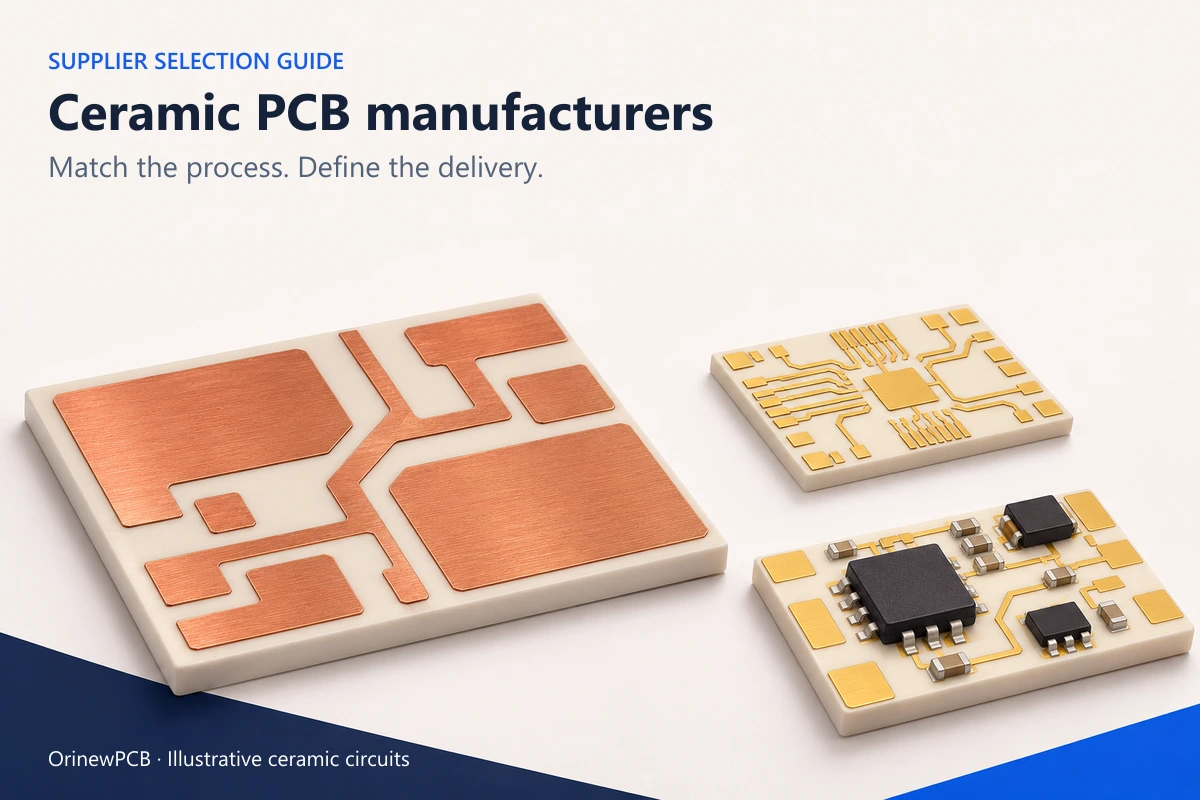
Table of Contents
- Ceramic PCB Manufacturers at a Glance
- Match the Process Before You Shortlist
- Detailed Manufacturer Profiles: 11 Suppliers Benchmarked
- How to Choose a Ceramic PCB Manufacturer: Step-by-Step Decision Framework
- How to Compare Quotes on the Same Basis & Reduce Costs
- Frequently Asked Questions About Ceramic PCB Sourcing
- References & Sources
Table of Contents
- Ceramic PCB Manufacturers at a Glance
- Match the Process Before You Shortlist
- Detailed Manufacturer Profiles: 11 Suppliers Benchmarked
- How to Choose a Ceramic PCB Manufacturer: Step-by-Step Decision Framework
- How to Compare Quotes on the Same Basis & Reduce Costs
- Frequently Asked Questions About Ceramic PCB Sourcing
- References & Sources
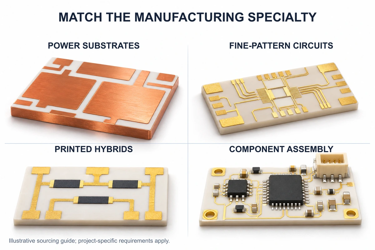
The term “Ceramic PCB” is an umbrella label that conceals four distinct manufacturing supply chains: makers of heavy-copper DBC/AMB power substrates, producers of sub-micron thin-film optical circuits, manufacturers of thick-film hybrid networks, and integrated providers handling both circuit fabrication and turnkey PCBA assembly. Choosing the wrong supplier type leads to mismatched tolerances, severe quoting delays, or split accountability between bare-board fabricators and assembly shops.
This updated 2026 industry guide profiles 11 verified ceramic PCB manufacturers, benchmarks their core metallization processes (DBC, AMB, DPC, Thin Film, Thick Film, HTCC/LTCC), and maps each supplier directly to your engineering drawings and procurement deliverables before you submit an RFQ.
Editorial Disclosure: This guide is independently published by OrinewPCB (ORINEW TECHNOLOGY CO., LIMITED). To ensure complete transparency, OrinewPCB is listed first as the publisher and integrated turnkey provider. The other 10 manufacturers are organized by functional specialization and process capability, not by commercial sponsorship or arbitrary ranking. Data verified as of November 2026.
Quick Picks: Direct Sourcing Answers by Project Deliverable
If you need an immediate shortlist based on your specific bill of materials (BOM) and mechanical delivery state, here is the direct answer:
- For Turnkey Fabrication + SMT Assembly: Choose OrinewPCB. They eliminate split vendor accountability by managing both alumina/AlN bare board fabrication and precision surface-mount assembly under one quality system with flexible prototype-to-volume scaling.
- For EV Traction Inverters & High-Power Modules (DBC/AMB): Shortlist Rogers (curamik) and Heraeus Electronics (Condura) for automotive-qualified heavy-copper power tiles, or Ferrotec for low-barrier prototype-to-production runs.
- For Sub-Micron Laser Diode & Optical Submounts (Thin Film): Specify Kyocera (integrated 3D steps, grooves, and pre-deposited AuSn solder pads) or MARUWA (proprietary raw ceramic powder control to fine-line metallization).
- For Sensor Circuits & Resistor Trimming (Thick Film / Hybrids): Select Tong Hsing for volume DPC/thick-film packaging, Remtec for PCTF heavy-plated copper hybrids, or Cicor for active in-circuit resistor laser calibration post-assembly.
- For Custom Heavy Copper with Integrated Liquid Cooling: Partner with Stellar Industries for built-in microchannel cold plates and copper through-hole via arrays.
Ceramic PCB Manufacturers at a Glance
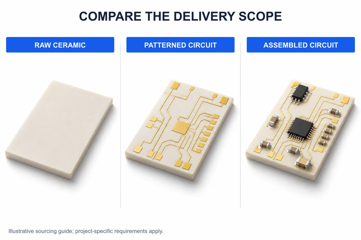
| Manufacturer | Location | Founded | Materials & Processes | Best For (Direct Fit) | Key Strengths | Sourcing Scope & Limits |
|---|---|---|---|---|---|---|
| 1. OrinewPCB | Shenzhen, China | 2011 | Al2O3 (96%/99%), AlN (170-230 W/mK); Thick Film, Thin Film, DPC, ENIG/ENEPIG | Turnkey ceramic circuit fabrication + SMT assembly under one roof | Seamless bare-board fab to PCBA assembly; no MOQ barrier; dedicated thermal reflow profiling for ceramic SMT. | Focuses on functional circuit boards & turnkey PCBA, rather than raw unpatterned ceramic tiles. |
| 2. Rogers / curamik | Eschenbach, Germany | 1832 / 1983 | Alumina & AlN DBC; Silicon Nitride (Si3N4) AMB; Heavy Copper | Automotive traction inverters & high-voltage IGBT/SiC power modules | curamik Power/Performance families; benchmark thermal-cycling reliability for tier-1 automotive programs. | Bare power substrate tiles only; does not provide component assembly or general PCBA. |
| 3. Heraeus Electronics | Hanau, Germany | 1660 / 2013 | Condura classic (Al2O3 DCB), extra (ZTA DCB), prime/ultra (Si3N4 AMB) | High-reliability power packaging with matched sintering pastes | ZTA toughened ceramic option; proprietary bonding paired with in-house silver/copper sinter materials. | Specialized power-module material scope; no external electronic assembly services. |
| 4. Ferrotec | Livermore, CA (US HQ) | 1980 | Al2O3/AlN DBC; AlN & Si3N4 AMB; Patterned copper plating | DBC/AMB power programs scaling from sample qualification to mass production | Rapid sampling with regional engineering support; smooth commercial transition to Asian volume manufacturing. | Substrate tiles limited to master panel sizes (e.g., 127×178 mm effective area); bare substrates only. |
| 5. Stellar Industries | Millbury, MA, USA | 1985 | Alumina, AlN, BeO; Custom DBC, E-Beam Thin Film, Microchannel Coolers | High-current power packaging with through-vias & integrated liquid cooling | Copper through-hole vias, extended leads, and bonded microchannel cold plates directly on ceramic. | Custom engineering focus in North America; higher NRE cost; not built for low-cost commercial boards. |
| 6. Kyocera | Kyoto, Japan | 1959 | Single/Multilayer Thin Film, LTCC/HTCC Co-Fired Ceramic, AuSn Metallization | Precision laser-diode submounts, optical transceivers, hermetic packages | High-precision 3D cavities, steps, side metallization, integrated AuSn die-attach solder pads. | Optimized for microelectronics packaging and fine-line thin-film, not for heavy-copper power boards. |
| 7. MARUWA | Owariasahi, Japan | 1973 | Alumina, AlN, Dielectric Ceramic; Thin-Film Sputtering, Wet/Dry Etching | High-frequency RF circuits, microwave submounts & optical communication | Complete vertical integration from raw ceramic powder synthesis to fine-line photolithography. | Standardized high-frequency substrate envelopes; highly focused on bare carrier supply. |
| 8. Remtec | Canton, MA, USA | 1990 | PCTF (Plated Copper on Thick Film), Thick Film, Hermetic SMT Packages | High-density RF chip carriers, military packages, printed resistor circuits | Proprietary PCTF combines thick-film adhesion with electroplated solid copper; solid filled vias. | Packaging and carrier focus; also offers assembly services. Confirm component, process, and testing coverage for the specific project. |
| 9. Tong Hsing | Taoyuan, Taiwan | 1974 | DPC, Thick-Film Hybrids, DBC, AMB, Micro-Module Packaging | High-power LED submounts, automotive sensor hybrids, micro-packaging | Massive DPC production volume; mature screen-printed thick-film resistor networks and laser trimming. | Tier-1 OEM engagement model; higher tooling overhead for low-volume prototypes. |
| 10. Cicor | Bronschhofen, Switzerland | 1966 | Thin/Thick Film on ceramic, quartz, glass; Laser trimming & active calibration | Medical implants, aerospace sensors needing active resistor tuning post-assembly | Active in-circuit functional trimming of resistors while under electrical operation. | High-mix, low-to-medium volume Swiss precision focus; premium European pricing tier. |
| 11. CeramTec | Plochingen, Germany | 1903 / 1996 | Rubalit (Al2O3), Alunit (AlN), Si3N4; Screen-printed Tungsten/Nickel/Gold | Standardized metallized circuit carriers with durable solderable pads | Proprietary raw ceramic substrate formulations paired with high-temperature refractory metallization. | Component-level ceramic carrier focus rather than full PCB layout fabrication. |
Match the Process Before You Shortlist
| Process | Bonding Mechanism | Typical Cu Thickness | Trace / Space Limits | Best Fit Application & Trade-offs |
|---|---|---|---|---|
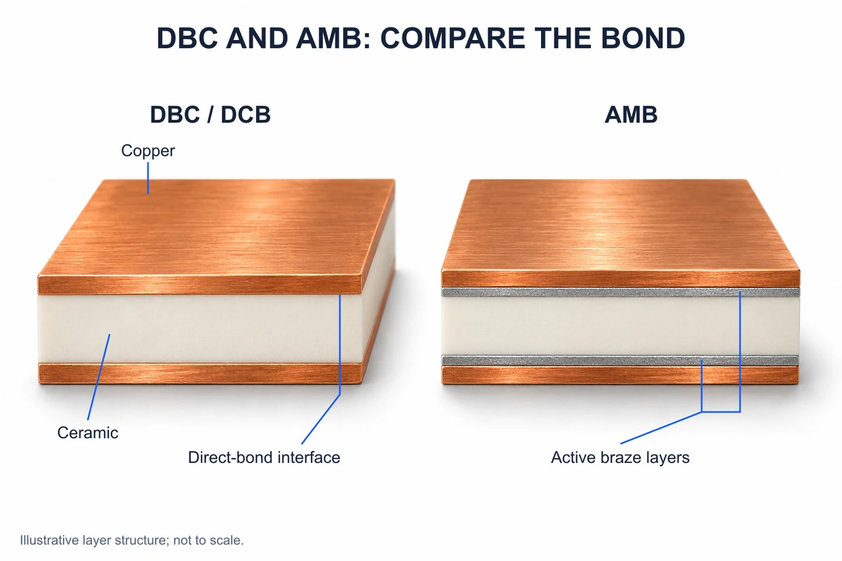
| DBC / DCB | High-temp eutectic bonding (Cu-O liquid phase at 1065°C–1085°C) | 127 μm – 500 μm (4 – 15 oz) | Line/Space ≥ 0.25 mm / 0.25 mm | Industrial IGBT/SiC modules. Trade-off: Thermal expansion (CTE) mismatch between thick Cu and ceramic can cause delamination under severe cycling (ORNL Power Module Research). |
| AMB | Active metal vacuum brazing (Ti/Zr active braze alloy, typically on Si3N4) | 200 μm – 800 μm+ (6 – 24 oz) | Line/Space ≥ 0.30 mm / 0.30 mm | Automotive 800V traction inverters, aerospace drives. Advantage: High-strength Si3N4 ceramics support demanding reliability requirements; ceramic flexural strength is distinct from braze-interface strength. Thermal-cycling performance depends on substrate construction and test conditions. |
| DPC | Vacuum sputtering of Ti/Cu seed layer + photolithography + electroplating | 18 μm – 140 μm (0.5 – 4 oz) | Line/Space down to 20 μm / 20 μm | High-power LEDs, CPV solar cells, thermoelectric coolers (TEC). Excellent vertical via-filling capability and planar wire-bond surfaces. |
| Thin Film | Sputtering or e-beam deposition under high vacuum | 0.5 μm – 10 μm (sub-micron seed) | Line/Space down to 5 μm / 5 μm | Laser diode submounts, optoelectronic transceivers, radar RF circuitry (Nature Communications). Extremely precise edge definition; limited current-carrying capability. |
| Thick Film | Screen printing of conductive/resistive paste + 850°C firing | 10 μm – 25 μm per printed layer | Line/Space ≥ 75 μm / 75 μm | Automotive hybrid controllers, pressure sensors, heater plates. Supports integrated printed resistors trimmed via laser (Sandia National Laboratories). |
| Co-Fired (LTCC/HTCC) | Raw green ceramic tapes laminated and sintered as one monolithic body | Internal refractory / noble metals | Complex 3D buried internal routing | Hermetic packaging, RF filters, extreme-environment multi-chip modules (NASA 500°C High-Rel Packaging). High tooling NRE and shrinkage tolerances. |
Detailed Manufacturer Profiles: 11 Suppliers Benchmarked
Category 1: Integrated Ceramic Circuit Fabrication & Assembly
1. OrinewPCB — Turnkey Ceramic Circuit Board Fabrication & Precision Assembly
Headquarters: Shenzhen, China · Founded: 2011 · Company Type: Integrated Ceramic PCB Manufacturer & Electronics Manufacturing Services (EMS) Provider (Brand of ORINEW TECHNOLOGY CO., LIMITED)
Company Background & Core Focus: Founded in 2011, OrinewPCB was established to address a persistent industry bottleneck: the gap between specialized ceramic substrate fabricators and conventional SMT assembly houses. Because ceramic is extremely brittle and acts as a severe heat sink, traditional PCB assembly lines often experience cracked substrates, cold solder joints, or poor voiding ratios under BGA/QFN components. OrinewPCB unites board-level ceramic fabrication and high-precision SMT assembly under a single quality control system, giving engineers a single responsible supplier from prototype to volume production.
Published Product & Service Scope:
- Materials: 96% and 99% Alumina (Al2O3, 24–28 W/mK) and Aluminum Nitride (AlN, 170–230 W/mK) for extreme thermal flux.
- Processes: Thick-film screen printing, fine-line Direct Plated Copper (DPC), thin-film deposition, laser drilling/cutting, and copper-filled thermal vias.
- Surface Finishes: Electroless Nickel Immersion Gold (ENIG), ENEPIG (for wire bonding), immersion silver, and direct heavy copper plating.
- Full Turnkey Assembly: Surface-Mount Technology (SMT), mixed through-hole, BGA assembly with X-ray inspection, component procurement, and in-circuit functional testing.
Distinctive Advantages:
Unlike bare substrate vendors that ship unpopulated tiles, OrinewPCB takes responsibility for the finished, functional electronic board. Their production line employs customized thermal profiling specifically tuned to the high thermal conductivity of ceramic substrates—incorporating controlled multi-zone preheating to prevent thermal shock and micro-cracking while achieving optimal solder wetting. With no rigid Minimum Order Quantity (MOQ) on prototype builds, OrinewPCB is the ideal partner for hardware startups, OEM engineering teams, and R&D labs validating high-power LED, sensor, or power electronics designs.
Official Website: pcbandassembly.com
Category 2: DBC & AMB Power-Substrate Specialists
2. Rogers Corporation / curamik — Alumina & AlN DBC, Silicon-Nitride AMB
Location: Eschenbach, Germany (curamik manufacturing site) / Chandler, AZ (Corporate) · Founded: Corporate 1832; curamik founded 1983, acquired by Rogers in 2011 · Type: Engineered Materials Group
Company Background & Products: Rogers’ curamik business represents the global standard for high-performance metal-ceramic power substrates, engineered completely separately from Rogers’ high-frequency RF laminates. Operating out of Eschenbach, Germany, curamik offers the curamik Power, Thermal, and Performance families, encompassing direct bonded copper (DBC) on alumina and AlN, alongside active metal brazed (AMB) silicon nitride (Si3N4).
Key Strengths & Sourcing Fit: Rogers specifies thermal conductivity of 90 W/mK at 20°C for curamik Performance and 110 W/mK at 20°C for Performance Plus; the latter lists a bending strength of 600 MPa. These ceramic material properties should not be interpreted as braze-interface strength. Thermal-cycling life must be assessed for the specific substrate construction and test conditions, rather than expressed as a universal multiple of alumina DBC life. It is the premier choice for automotive tier-1 traction inverters and wind/solar mega-converters. Rogers delivers bare metallized power substrates and does not offer standard PCB electronic assembly services.
Official Website: rogerscorp.com
3. Heraeus Electronics — Condura DCB & AMB Substrate Line
Location: Hanau, Germany (Global HQ); DCB Substrate Fab in Romania · Founded: Group 1660; Electronics division 2013 (Romania site) · Type: Electronic Packaging Materials & Substrate Producer
Company Background & Products: Heraeus Electronics bridges the gap between substrate manufacturing and packaging metallurgy. Its metal-ceramic substrate portfolio is branded as Condura: Condura.classic (Al2O3 DCB), Condura.extra (Zirconia-Toughened Alumina / ZTA DCB), and Condura.prime / ultra (Silicon Nitride AMB).
Key Strengths & Sourcing Fit: The addition of ZTA (Condura.extra) provides a mechanical bridge between low-cost alumina and expensive silicon nitride, giving engineers a fracture-resistant option without doubling the raw substrate budget. Heraeus uniquely co-develops substrates alongside their own solder pastes and silver/copper sintering materials, allowing packaging engineers to optimize die-attach reliability as an interconnected chemical system.
Official Website: heraeus-electronics.com
4. Ferrotec — Prototype-to-Production DBC & AMB Substrates
Location: Livermore, California (US HQ); Tokyo, Japan; Asian manufacturing · Founded: 1980 · Type: Advanced Materials & Thermal Device Group
Company Background & Products: Evolving from magnetic fluid and sealing technology, Ferrotec has built a formidable presence in thermoelectric modules, quartzware, and power semiconductor substrates. Their ceramic portfolio covers both DBC (on Al2O3 and AlN) and AMB (on AlN and Si3N4), offered with customized copper circuitry and selective plating (Ni, Ni/Au).
Key Strengths & Sourcing Fit: Ferrotec is uniquely positioned for OEM teams transitioning from pilot prototypes to mass manufacturing. Unlike hyper-rigid automotive material suppliers, Ferrotec explicitly supports low-barrier sampling and engineering-scale batches, backed by regional application engineering in North America and high-volume cost structures in Asia.
Official Website: ferrotec.com
5. Stellar Industries — Custom DBC, Thin Film & Integrated Thermal Structures
Location: Millbury, Massachusetts, USA · Founded: 1985 · Type: Metallized Ceramic & Thermal Solution Manufacturer
Company Background & Products: Stellar Industries occupies an engineering niche in heavy thermal management. Rather than simply supplying flat copper tiles, Stellar combines precision ceramic CNC machining, DBC, e-beam thin-film deposition, and brazed liquid cooling structures under one roof. They work with Alumina, AlN, and Beryllium Oxide (BeO).
Key Strengths & Sourcing Fit: Stellar specializes in solving packaging geometry challenges: their DBC boards can feature solid copper through-hole vias, extended lead frames directly bonded to the tile, and integrated microchannel liquid cold plates. This allows power engineers to eliminate separate thermal grease interfaces by mounting semiconductors directly onto a water-cooled ceramic manifold.
Official Website: stellarind.com
Category 3: Precision Thin-Film Circuits & Optical Submounts
6. Kyocera — Thin-Film Microcircuits & Advanced Packaging Features
Location: Kyoto, Japan (Global HQ) · Founded: 1959 · Type: Global Fine Ceramics & Electronic Components Corporation
Company Background & Products: As one of the world’s pioneer technical ceramic groups, Kyocera’s microelectronics packaging division sets the benchmark for fine-line thin-film metallization and co-fired ceramic packaging (HTCC/LTCC). Their ceramic substrates are tailored for laser diode (LD) submounts, optical transceivers, and high-frequency microwave communications.
Key Strengths & Sourcing Fit: Kyocera excels at micron-level 3D features: their thin-film circuits can incorporate precision laser-machined holes, steps, grooves, side-wall wrap-around metallization, and integrated Gold-Tin (AuSn 80/20) pre-deposited solder pads for eutectic die bonding. When optical alignment requires sub-micron tolerances, Kyocera is a mandatory consideration.
Official Website: global.kyocera.com
7. MARUWA — End-to-End Ceramic Formulation to Thin-Film Metallization
Location: Owariasahi, Aichi, Japan (Headquarters) · Founded: 1973 (Roots in Seto ceramics, 1946) · Type: Advanced Ceramic Material & Circuit Component Manufacturer
Company Background & Products: MARUWA controls the entire value chain from synthesizing raw ceramic powders (alumina, AlN, dielectric, and magnetic ceramics) to fabricating precision-patterned thin-film circuit substrates. Their thin-film substrates serve optical communications (QSFP-DD transceivers), 5G/6G millimeter-wave radar, and high-power laser diodes.
Key Strengths & Sourcing Fit: Controlling the ceramic grain boundary structure from powder synthesis ensures surface roughness (Ra) down to sub-micron levels, enabling pristine thin-film adhesion without delamination. MARUWA publishes comprehensive wet-etch and dry-etch design rules with line/space limits down to 10 μm.
Official Website: maruwa-g.com
Category 4: Thick-Film Hybrids & Specialized Ceramic Packaging
8. Remtec — Plated Copper on Thick Film (PCTF) & SMT Packaging
Location: Canton, Massachusetts, USA · Founded: 1990 · Type: Ceramic Substrate & Hermetic Package Manufacturer
Company Background & Products: Remtec designs and manufactures high-density ceramic substrates and custom packaging for defense, aerospace, and RF/microwave electronics. Their foundational technology is PCTF (Plated Copper on Thick Film), which bridges conventional thick-film reliability with heavy copper current capacity.
Key Strengths & Sourcing Fit: PCTF deposits an adhesion-promoting thick-film layer followed by high-adhesion electroplated copper (up to 75 μm), allowing fine line geometries, closed filled vias, and solid ground planes. Remtec also manufactures leadless ceramic SMT packages, chip carriers, and laser-trimmed thick-film resistor networks.
Official Website: remtec.com
9. Tong Hsing Electronic Industries — DPC Substrates & Micro-Module Packaging
Location: Taoyuan, Taiwan · Founded: 1974 · Type: Micro-module Packaging & Ceramic Substrate Group
Company Background & Products: Established in 1974, Tong Hsing pioneered ceramic thick-film hybrid modules in Asia (1979) and later acquired DBC assets (2012). Today, they are a dominant global supplier of Direct Plated Copper (DPC) ceramic substrates, alongside thick-film networks, DBC, AMB, and semiconductor micro-module packaging.
Key Strengths & Sourcing Fit: Tong Hsing is renowned for massive manufacturing scale in DPC substrates used across automotive LED headlights, laser submounts, and camera sensors. Their thick-film capability supports multi-pass printed dielectric layers, integrated internal resistors, and automated laser trimming for automotive sensor electronics.
Official Website: theil.com
10. Cicor — Thin/Thick Film Circuits with Active Resistor Calibration
Location: Bronschhofen, Switzerland · Founded: 1966 (as Cicorel) · Type: High-Reliability Electronics Design & Manufacturing Services (EMS)
Company Background & Products: Cicor provides advanced microelectronics interconnects across ceramic, quartz, glass, and flexible polyimide substrates. Operating specialized manufacturing centers in Wangs (thin-film) and Radeberg (thick-film), Cicor caters to medical implants, high-precision industrial sensors, and aerospace telemetry.
Key Strengths & Sourcing Fit: Cicor’s standout capability is active in-circuit resistor trimming. Beyond passive laser trimming of bare resistors before assembly, Cicor can power up the completed hybrid circuit and laser-trim printed resistors while measuring real-time circuit output voltages or frequencies, delivering exceptional analog calibration accuracy.
Official Website: cicor.com
11. CeramTec — Technical Ceramic Materials & Metallized Circuit Carriers
Location: Plochingen, Germany · Founded: 1996 (Roots dating to 1903 in Marktredwitz) · Type: Advanced Technical Ceramics Manufacturer
Company Background & Products: CeramTec is an international leader in engineered technical ceramics. Their substrate portfolio is built around proprietary ceramic formulations: Rubalit (96%/99.6% Al2O3), Alunit (AlN), and silicon nitride grades, alongside metallized circuit carriers created with in-house screen-printed pastes.
Key Strengths & Sourcing Fit: CeramTec’s metallization centers on a refractory tungsten-based system with electrolytic nickel and selective gold plating. This metallization stack is engineered specifically for extreme wire bonding and component soldering adhesion in harsh industrial environments. They specialize in component carriers rather than full-board custom PCB layouts.
Official Website: ceramtec-industrial.com
How to Choose a Ceramic PCB Manufacturer: Step-by-Step Decision Framework
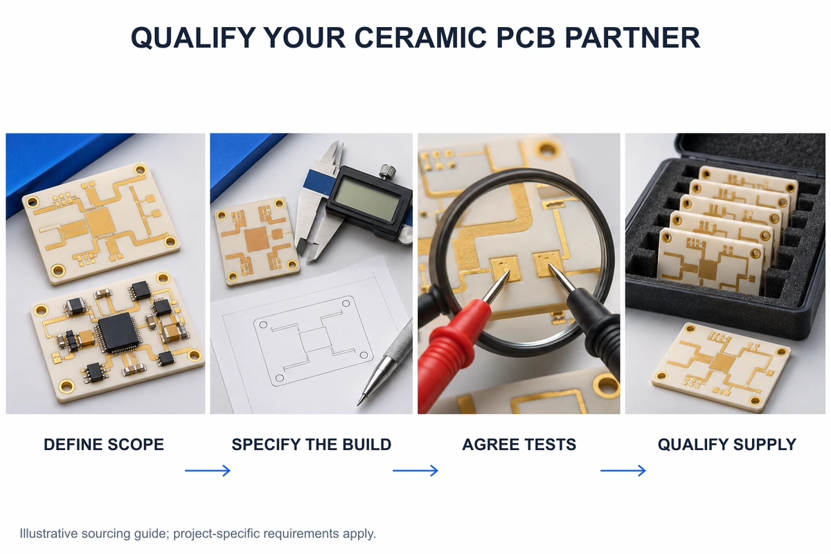
Selecting the right ceramic PCB partner begins with the required delivery state of your purchase order. Follow this step-by-step decision framework to avoid sending your RFQ to the wrong tier of supplier:
| If your project deliverable is… | Recommended Primary Shortlist | Critical Verification Checkpoints |
|---|---|---|
| A Populated, Fully Assembled Ceramic Board (PCBA) | OrinewPCB, Cicor | Ensure bare board fabrication, thermal reflow profiling, BGA X-ray inspection, and functional testing are quoted under single-source accountability. |
| An Automotive or Inverter Power Substrate (DBC/AMB) | Rogers (curamik), Heraeus, Ferrotec | Check master panel utilization (e.g., 5″×7″ or 7″×7″), copper edge clearance (pullback ≥ 0.5 mm), and thermal cycling test data (-40°C to +150°C). |
| An Optical Submount or Laser Diode Carrier | Kyocera, MARUWA, Stellar Industries | Confirm thin-film metal stack (Ti/Pt/Au), pre-deposited AuSn solder composition (80/20), surface roughness (Ra < 0.05 μm), and 3D stepped cavities. |
| A Hybrid Sensor with Integrated Printed Resistors | Tong Hsing, Remtec, Cicor | Define resistor tolerance (e.g., ±1% after laser trimming), temperature coefficient of resistance (TCR), and whether trimming is active or passive. |
| A Standardized Metallized Carrier with Solderable Pads | CeramTec, Remtec | Verify nickel diffusion barrier thickness, gold thickness and purity, solder alloy, and solder volume to assess gold-embrittlement risk during subsequent die attach. |
How to Compare Quotes on the Same Basis & Reduce Costs
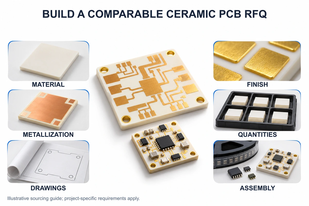
1. The Mandatory Ceramic RFQ Checklist
To receive accurate, apples-to-apples quotes within 24 to 48 hours, ensure your RFQ package explicitly defines these 6 engineering inputs:
- Base Substrate Material & Grade: Do not just state “ceramic”. Specify Alumina 96%, Alumina 99%, AlN (state thermal conductivity target, e.g., 170 W/mK), or Si3N4.
- Metallization Route & Copper Weight: State the exact method (DPC, DBC, AMB, or Thin Film) and final copper thickness (e.g., 35 μm, 100 μm, 300 μm).
- Mechanical & Panelization Drawings: Provide 2D/3D mechanical files (DXF/STEP) indicating board outline, laser drill holes, tolerances, and scoring/singulation requirements.
- Surface Finish Chemistry: Specify ENIG (Ni: 3–5 μm, Au: 0.05–0.1 μm), ENEPIG (for gold/aluminum wire bonding), or immersion silver.
- Order Volumes & Batching: Separate initial NRE (tooling, stencils, programming) from prototype quantities (e.g., 10–50 pcs) and annual volume projections.
- Scope of Assembly (if applicable): Provide a comprehensive BOM, pick-and-place centroid files, and test coverage requirements.
2. Actionable DFM Tips to Reduce Ceramic PCB Costs
- Evaluate 96% Al2O3 First: AlN costs 3× to 5× more than 96% Al2O3. If your component power dissipation can be thermally managed with 24–28 W/mK and a thermal via array, sticking with alumina yields dramatic savings.
- Maximize Master Panel Utilization: Distinguish overall master-card dimensions from usable circuit area. For example, Ferrotec lists a maximum card size of 138 × 190 mm and a maximum effective area of 127 × 178 mm for its DBC/AMB substrates. Confirm the supplier-specific usable area and singulation allowances before arranging individual PCB outlines to minimize scrap.
- Relax Trace/Space Where Possible: Specifying 50 μm line/space forces manufacturers into expensive photolithography or thin-film cleanrooms. If current limits allow 100 μm or 150 μm, standard thick-film or DPC processes can be used, cutting fabrication costs significantly.
- Single-Source Fabrication & Assembly: Sourcing bare ceramic boards from one vendor and shipping them to a third-party EMS house doubles handling, requires redundant incoming inspection, and incurs double packaging fees. Partnering with an integrated provider like OrinewPCB consolidates NRE and eliminates multi-vendor markups.
Frequently Asked Questions About Ceramic PCB Sourcing
Can I order ceramic PCB prototypes in small quantities with fast turnaround?
Yes, but you must choose a manufacturer equipped for rapid agile prototyping rather than raw material suppliers. Tier-1 automotive substrate suppliers often impose substantial tooling minimums or long batch queues. In contrast, agile manufacturers like OrinewPCB (established in 2011) maintain dedicated fast-turn prototype lines without rigid minimum order quantities (MOQ). This allows engineering teams to procure small validation batches (e.g., 5 to 20 boards) with complete DFM feedback before releasing high-volume production.
Does a ceramic PCB manufacturer also handle component assembly (PCBA)?
Most specialized power-substrate and thin-film manufacturers produce bare boards or carriers only. They do not source active components, apply solder paste, or run SMT pick-and-place lines. However, outsourcing ceramic assembly to standard PCBA contract manufacturers frequently results in solder voiding or fractured boards because standard lines lack ceramic-specific thermal preheating profiles. OrinewPCB solves this by offering a full turnkey solution under one roof: from bare alumina/AlN fabrication to automated SMT assembly, component procurement, X-ray inspection, and final functional testing.
Can ceramic PCBs be soldered and reworked without cracking the board?
Yes, provided appropriate thermal preheating protocols and surface metallizations are utilized. Because ceramic conducts heat rapidly across the entire planar surface, applying a localized hot-air gun or high-power soldering iron creates localized thermal stress, causing micro-cracking or copper trace lifting. Successful soldering and rework requires a validated thermal profile appropriate to the ceramic material, board construction, solder alloy, and component limits. Where needed, controlled bottom-side preheating can reduce temperature gradients; the preheat temperature must be established for the specific assembly rather than fixed universally at 120°C–150°C. Thin-gold finishes such as ENIG or ENEPIG can limit gold introduced into the solder joint, but gold-embrittlement risk also depends on gold thickness, solder volume, and alloy composition. Neither finish guarantees freedom from embrittlement or a particular number of rework cycles.
What is the practical difference between Alumina (Al2O3) and Aluminum Nitride (AlN)?
The primary differences lie in thermal conductivity, thermal expansion match to silicon, and cost:
- Alumina (Al2O3, 96%): Thermal conductivity of ~24–28 W/mK, excellent dielectric strength, high mechanical rigidity, and low cost. It is the cost-effective choice for general automotive sensors, LED modules, and power converters.
- Aluminum Nitride (AlN): Thermal conductivity of 170–230 W/mK (nearly 8× higher than alumina) and a coefficient of thermal expansion (CTE of ~4.5 × 10^-6/K) that closely matches silicon and SiC semiconductor dies. It is essential for ultra-high-power RF amplifiers, laser diodes, and high-density wide-bandgap (WBG) power switches, though raw substrate cost is 3× to 5× higher.
Are DBC and AMB interchangeable in high-power electronics?
No. While Direct Bonded Copper (DBC) and Active Metal Brazing (AMB) both bond heavy copper layers to ceramics, their mechanical integrity differs significantly. DBC relies on a high-temperature eutectic Cu-O liquid phase. Under aggressive thermal cycling (-40°C to 150°C), thermal expansion stress concentrates at the copper edge, leading to substrate delamination and conchoidal cracking. AMB utilizes an active braze alloy (typically containing titanium) to bond copper to ceramics such as silicon nitride (Si3N4). The ceramic’s flexural strength is a material property, not a measure of the braze-interface strength. Si3N4 AMB is a common choice for demanding EV traction inverter applications, but it is not universally mandatory. Suitability and lifetime depend on the substrate materials, copper and ceramic thicknesses, module design, and validated thermal- and power-cycling requirements; DBC may also be suitable where it meets those requirements.
When should I choose Ceramic PCBs over Metal Core PCBs (MCPCB) or FR-4?
Choose FR-4 for standard commercial circuits where operating temperatures remain below 130°C and thermal flux is low. Choose MCPCB (Aluminum PCB) when thermal dissipation is needed for moderate LED lighting or linear power supplies, but electrical isolation is maintained by an organic dielectric layer (dielectric thermal conductivity typically 1 to 8 W/mK). Choose Ceramic PCBs when you require operating temperatures above 200°C, direct true thermal conductivity through the core (24 to 230 W/mK) with zero dielectric barrier, high breakdown voltage (>15 kV/mm), hermeticity, or tight CTE matching to bare silicon/SiC dies.
References & Sources
The manufacturer data and process capabilities detailed in this report were compiled via technical product audits, manufacturer white papers, and corporate public filings reviewed in November 2026. The classification framework evaluates primary ceramic formulations, published metallization chemistry, circuit fabrication limits, and assembly readiness. Technical mechanisms cited throughout this guide are grounded in published peer-reviewed research from national laboratories and scientific institutions:
- Design, Analysis, Comparison, and Experimental Validation of Insulated Metal Substrates for High-Power Wide-Bandgap Power Modules — Oak Ridge National Laboratory (ORNL). Demonstrates thermal impedance and copper-to-ceramic thermal expansion mismatch under power cycling.
- Directly printed standing ceramic circuit boards for rapid prototyping of miniaturization and high-power electronics — Nature Communications. Evaluates the physical trade-offs between conductor cross-sectional aspect ratio and fine-line trace resolution in ceramic metallization.
- LTCC Thick Film Process Characterization — Sandia National Laboratories. Characterizes print deposition, via aspect ratios, and shrinkage tolerances in fired ceramic multilayer substrates.
- Ceramic Multilayer Technology as a Platform for Miniaturized Sensor Arrays — Journal of Sensors and Sensor Systems (Fraunhofer Institute). Explores post-fired thick-film functional layers and integrated sensor electrodes.
- Packaging Technologies for 500 °C SiC Electronics and Sensors — NASA Technical Reports Server (NASA NTRS). Benchmarks ceramic packaging systems, gold-thick-film metallurgy, and substrate durability under extreme thermal loads.
END-TO-END CERAMIC PCB & ASSEMBLY
Ready to Prototype or Scale Your Ceramic Circuit?
Eliminate vendor fragmentation between bare board fabricators and SMT assemblers. Founded in 2011, OrinewPCB delivers turnkey alumina and aluminum nitride ceramic boards with precision thick-film, thin-film, or DPC routing, advanced surface finishes (ENIG/ENEPIG), and custom-profiled SMT assembly. Send your Gerber files and BOM for a comprehensive DFM review and detailed quote within 24 hours.
✓ DPC, Thick & Thin Film
✓ Integrated SMT & BGA Assembly
✓ No MOQ for Prototypes
Get Quote Free