8 RF PCB Manufacturers for Prototypes and Production
Compare eight RF PCB manufacturers for prototypes and production by materials, manufacturing capabilities, assembly scope and production transfer controls.
Get Your PCB Quote!

Table of Contents
Table of Contents
Sourcing RF and microwave PCBs requires more than finding a board shop that lists Rogers laminates on its capability sheet. A prototype that functions on the test bench can run into unexpected insertion loss or impedance shifts during volume production if the manufacturer alters the copper foil profile, substitutes bondply materials, changes etch compensation, or shifts the build to a secondary facility without proper qualification.
For hardware teams seeking an integrated China-based prototype-to-production route with bare-board fabrication and turnkey SMT assembly in a single procurement conversation, OrinewPCB provides high-frequency fabrication, stocked Rogers, Taconic, and PTFE laminates, hybrid stackup planning, and assembly support. Sierra Circuits and AdvancedPCB provide strong domestic US pathways from engineering prototypes to production builds. TTM Technologies and Summit Interconnect specialize in complex multilayer RF structures and advanced microwave interconnects, while American Standard Circuits leads in metal-backed PTFE thermal carriers and Schweizer Electronic specializes in automotive radar PCB industrialization.
Publisher Disclosure: OrinewPCB publishes this guide and is included as one of the options. This article is based on publicly available manufacturer documentation and engineering analysis; it does not constitute an endorsement, price comparison, or guarantee of supplier performance for a specific project.
Quick Picks by Sourcing Scenario
- China-Based RF Fabrication + Assembly: OrinewPCB — Combines RF bare-board manufacturing, stocked Rogers/Taconic/PTFE materials, hybrid stackup modeling, and turnkey SMT assembly under one supplier discussion.
- US RF Prototypes with a Production Route: Sierra Circuits — Operates two published US RF fabrication facilities with automated material scaling, in-house plasma/sodium PTFE hole conditioning, and turnkey Silicon Valley assembly.
- Complex RF Structures & Microwave Interconnects: TTM Technologies — Supports high-complexity architectures including PTFE fusion bonding, multi-level cavities, tight feature etch tolerances, and RF testing up to 110 GHz.
- RF + High-Speed Digital Hybrids (US): AdvancedPCB — Unites multiple US facilities with dedicated quick-turn RF lines up to 8 layers, fine-line etching down to 2.75 mil, and mixed RF/high-speed digital hybrid constructions.
- High-Reliability RF Multilayers & Waveguides: Summit Interconnect — Fabricates microwave boards built to IPC-6018 specifications, offering tight impedance control, mode-suppression vias, plated cavities, and S-parameter testing.
- Metal-Backed PTFE & Thermal RF Boards: American Standard Circuits (ASC) — Specializes in pre-bonded and post-bonded metal-backed PTFE laminates, sweat-solder bonding, CNC pocket machining, and wire-bond finishes.
- European Multi-Laminate & Radar Projects: Cistelaier — Offers European manufacturing with an extensive published library of Rogers, Taconic, Isola, Nelco, and specialty foam spacer substrates.
- Automotive 77 GHz Radar & Combi-Board Integration: Schweizer Electronic — Specializes in tight-tolerance 77 GHz antenna etching, asymmetric RF/digital hybrid stackups, and localized RF inlay Combi Boards.
RF PCB Manufacturers at a Glance
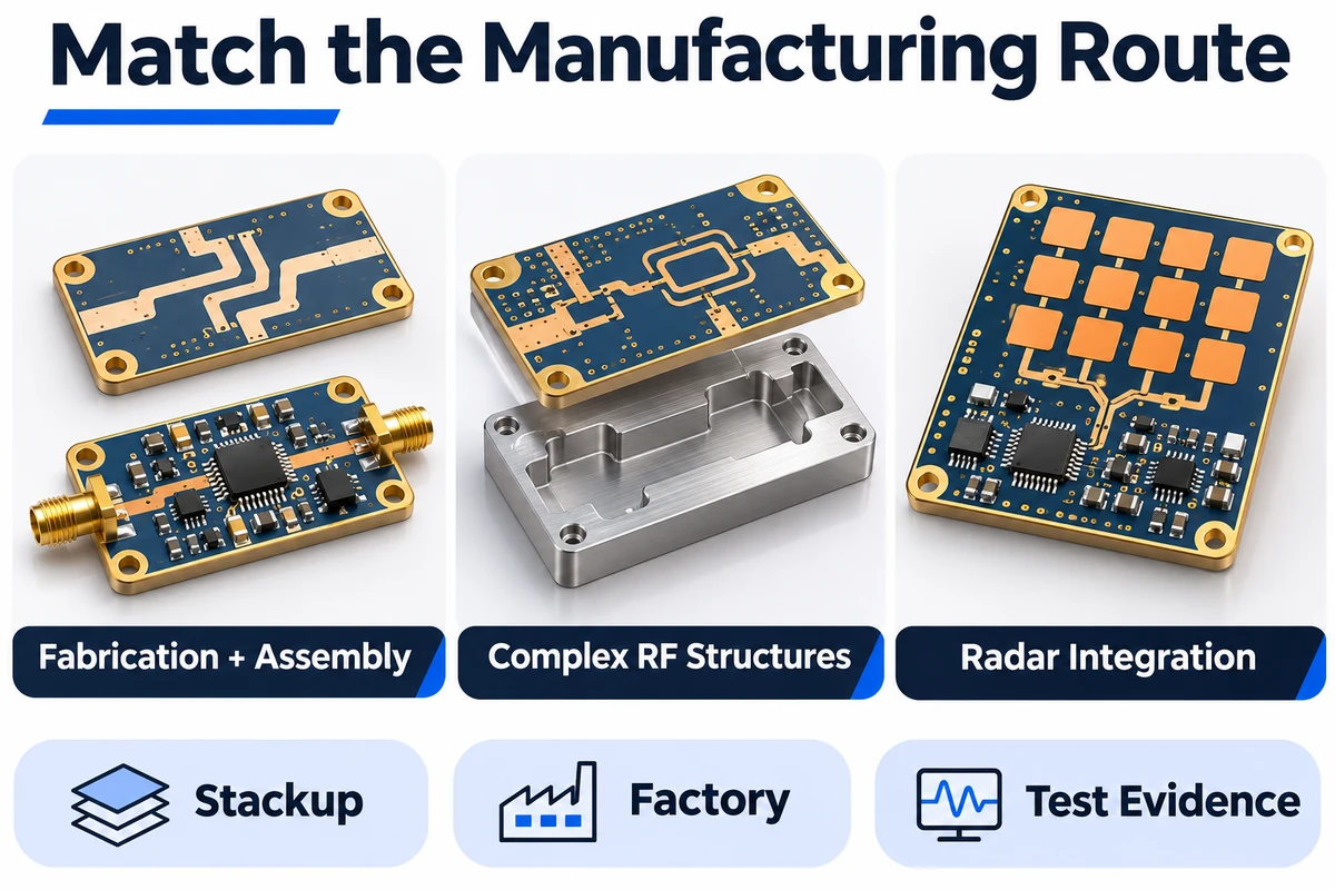
Selecting an RF PCB manufacturer starts with matching your board’s operating frequency, stackup complexity, thermal dissipation needs, and geographic requirements against each fabricator’s verified process capabilities.
| Manufacturer | Headquarters & Footprint | Founded | Core RF Capabilities & Services | Key Process & Technical Strengths | Best For |
|---|---|---|---|---|---|
| OrinewPCB | Shenzhen, China (Production allocation confirmed per quote) | 2011 | High-frequency PCBs, Rogers PCBs, PTFE/FR-4 hybrids, turnkey PCBA | Stocked Rogers/Taconic cores, LDI fine-line imaging, backdrilling, Polar SI9000 modeling, integrated SMT | China-based prototype-to-production RF projects needing integrated assembly |
| TTM Technologies | Santa Ana, CA, USA (Global multi-site network) | 1998 | RF/microwave PCBs (L to mmWave bands), RF assemblies, specialty interconnects | PTFE fusion bonding, multi-level cavities, tight etch tolerances, stub-removal backdrilling, 110 GHz RF test lab | Complex defense, aerospace, and mmWave programs requiring advanced RF cavity routing |
| Sierra Circuits | Sunnyvale, CA, USA (2 US RF facilities) | 1986 | RF/microwave prototypes, production boards, turnkey assembly | Automated XACT material scaling, plasma/sodium PTFE hole treatment, multi-cycle lamination | US engineering teams seeking fast-turn RF prototypes and domestic scaling |
| Summit Interconnect | California, USA (North American network) | 2016 | RF/microwave, HDI, flex/rigid-flex, thermal management PCBs | IPC-6018 microwave fabrication, tight stripline impedance, plated cavities/edges, bonded heat sinks | High-reliability North American RF multilayers with waveguide or cavity features |
| AdvancedPCB | United States (6 US facilities) | 1977 roots (2024 unified brand) | Quick-turn RF prototypes through production, high-speed hybrids, PCBA | Dedicated RF lines up to 8 layers, 2.75 mil trace/space, RF + high-speed digital hybrid constructions | US lower-to-mid layer count RF modules and mixed-dielectric digital/RF hybrids |
| American Standard Circuits | West Chicago, IL, USA (US + offshore alliances) | 1988 | RF/microwave, metal-backed PTFE, thermal carriers, flex/rigid-flex | Pre-bonded & post-bonded metal-core PTFE, sweat-solder bonding, CNC pocket machining, wire-bond finishes | High-power RF amplifiers and transmitters requiring integrated metal heat sinks |
| Cistelaier | Modena, Italy (Italian plants; Finmasi Group) | 1976 roots | Multilayer, HDI, flex/rigid-flex, RF/microwave, large-format radar PCBs | Broad European material library (Rogers, Taconic, Isola, Nelco), large-format radar boards up to 855 mm | European aerospace, defense radar, and telecom mixed-dielectric projects |
| Schweizer Electronic | Schramberg, Germany (Europe & Asia network) | 1849 roots (PCBs since 1958) | 6–24 GHz RF PCBs, 77 GHz radar PCBs, Combi Boards, power/embedding | Typical ±15 µm trace width control on 77 GHz radar antennas, asymmetric hybrids, localized RF inlays | Automotive ADAS radar sensors and high-volume industrial mmWave industrialization |
8 RF PCB Manufacturers Compared in Detail
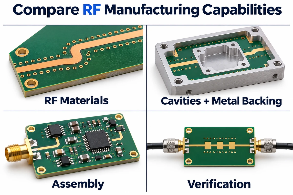
The eight manufacturers below represent distinct engineering specializations and supply-chain routes. Rather than treating them as interchangeable commodity vendors, evaluate each supplier by its lamination experience, impedance verification methods, and ability to preserve your approved prototype baseline into recurring production.
1. OrinewPCB — China-Based RF Fabrication and Turnkey Assembly
OrinewPCB provides PCB fabrication and assembly services for high-frequency and microwave projects from rapid prototyping into volume production. For hardware teams seeking to streamline supply chains, OrinewPCB combines RF bare-board fabrication, controlled-impedance stackup planning, and fine-pitch SMT assembly within a single engineering and procurement workflow.
RF Capabilities & Material Portfolio
- RF & Low-Loss Laminates: Fabricates high-frequency boards utilizing Rogers (including RO4003C, RO4350B, RO3003, RO3010, and RT/duroid series), Taconic, Arlon, and PTFE-based substrates, supported by dedicated high-frequency PCB manufacturing and Rogers PCB fabrication capabilities.
- Layer Count & Hybrid Constructions: Supports multilayer RF boards (standard 2 to 24 layers, with complex multilayer and hybrid configurations evaluated per design review) combining low-loss RF cores with High-Tg FR-4 digital/power layers to optimize electrical performance and panel economics.
- Fine-Line Trace & Impedance Control: Supports fine-line conductor imaging down to 3/3 mil (with tighter prototype capabilities subject to stackup review), controlled impedance modeling, and test coupon verification to ±10% (tight tolerance options available per engineering review).
- Integrated Prototype & Production Assembly: Through its prototype PCB service and turnkey assembly lines, provides SMT placement for RF transceivers, QFNs, and BGAs with optical and X-ray inspection, eliminating coordination friction between separate board fabricators and assemblers.
Key Strengths
- Provides an integrated route for RF bare-board manufacturing and SMT assembly under one roof, reducing development cycles and vendor handoff risks.
- Supports a broad range of verified low-loss laminate families and hybrid stackups tailored to commercial RF, telecommunications, and sensor applications.
Best Sourcing Fit: Commercial, telecom, automotive, and industrial hardware teams seeking a cost-effective China-based RF PCB and turnkey PCBA route with clear stackup and impedance verification.
Engineering & Sourcing Considerations: Confirm the exact laminate grade, copper foil type, test coupon deliverables, and production factory allocation in the formal quotation before freezing the build package.
2. TTM Technologies — Complex RF Structures and Advanced Interconnects
TTM Technologies is a major global manufacturer of advanced technology PCBs and RF/microwave assemblies. Its published RF portfolio focuses on mission-critical, high-reliability, and technically demanding architectures across frequencies extending from L/S bands into millimeter-wave spectrum.
RF Capabilities & Material Portfolio
- Tight Feature Tolerances: Publishes capabilities including tight etch tolerances (down to ±0.0005″ / ±12.7 µm on unplated 0.5 oz copper under specific process conditions) and precision front-to-back layer registration utilizing laser direct imaging.
- Specialty RF Processes: Supports complex microwave structures including pure PTFE fusion bonding (eliminating thermoplastic bonding films), sequential lamination, multi-level blind cavities, plated board edges/slots, and Ormet transient-liquid-phase sintered paste for z-axis interconnects.
- Via Optimization & Stub Removal: Offers mechanical backdrilling, laser drilling, and laser-modified controlled-depth drilling to minimize or eliminate resonant via stubs on high-speed RF transitions.
- Advanced RF Test & Lab Facilities: Maintains specialized RF test centers equipped with Vector Network Analyzers capable of frequency sweeps up to 110 GHz for material and S-parameter characterization, alongside 3D surface scanning for copper foil profile analysis.
Key Strengths
- Industry-leading expertise in exotic bonding processes like PTFE fusion bonding and cavity machining for integrated waveguide and filter structures.
- Comprehensive in-house RF characterization equipment supporting extreme frequency validation.
Best Sourcing Fit: Complex defense, aerospace, telecommunications, and millimeter-wave radar programs requiring advanced RF cavity routing, fusion-bonded multilayers, and specialized interconnects.
Engineering & Sourcing Considerations: Not every facility in TTM’s global network supports every published RF process or test frequency; buyers should confirm site-specific capabilities and qualifications for the quoted build.
3. Sierra Circuits — US RF Prototypes Through Volume Production
Sierra Circuits operates a dedicated Silicon Valley campus with two published RF fabrication facilities. Positioned around engineering collaboration and fast-turn delivery, Sierra provides online stackup modeling tools, automated process control, and turnkey assembly under domestic US manufacturing.
RF Capabilities & Material Portfolio
- RF Stackup & Lamination Range: Publishes RF manufacturing capabilities covering 2 to 30 layers, finished board thicknesses from 10 to 275 mil, minimum core and dielectric thicknesses down to 3 mil (0.0762 mm), and multi-cycle sequential lamination.
- PTFE Hole Conditioning & Scaling: Employs automated scaling software (XACT) to predict layer-by-layer material movement, alongside in-house plasma and sodium-etch chemical hole preparation to ensure reliable copper plating adhesion on PTFE hole walls.
- Conductor & Impedance Control: Delivers 3/3 mil trace/space geometry, controlled impedance tolerance to ±5% on qualified constructions, small mechanical drills (down to 5.9 mil), and controlled-depth backdrilling with tight depth tolerance.
- Laminate Range & Assembly: Processes low-loss substrates including Rogers RO4000/RO3000 series, Taconic, Isola Astra MT77 / I-Tera MT40, and Panasonic Megtron materials, combined with in-house fine-pitch SMT assembly down to 01005 passives and 0.35 mm pitch BGAs.
Key Strengths
- Strong domestic US quick-turn prototyping ecosystem with robust online DFM tools and integrated Silicon Valley assembly lines.
- Dedicated PTFE hole preparation (plasma and sodium etch) provides reliable barrel plating for challenging high-frequency laminates.
Best Sourcing Fit: US hardware teams requiring domestic fast-turn RF prototypes, collaborative DFM stackup support, and an established path to recurring production.
Engineering & Sourcing Considerations: Confirm which facility will manufacture prototype versus volume builds, and verify whether the quoted production route preserves identical laminate brands, stackups, and test deliverables.
4. Summit Interconnect — RF Multilayers and Specialty Cavities
Summit Interconnect is a major North American manufacturer of advanced PCBs serving aerospace, defense, telecommunications, and industrial electronics. Its RF and microwave services emphasize dense multilayer integration, precise CAM modeling, and thermal management.
RF Capabilities & Material Portfolio
- IPC-6018 Microwave Fabrication: Fabricates RF and microwave printed circuit boards built to IPC-6018 performance specifications, supporting tight-tolerance stripline, microstrip, and coplanar waveguide routing with controlled impedance held within ±5% on suitable builds.
- Mode Suppression & Cavity Features: Implements advanced via spacing and suppression techniques in dense RF layouts, alongside precision controlled-depth milling, plated cavities for embedded filters and drop-in components, and plated board edges for shielding.
- Thermal Dissipation Integration: Integrates metal-backed substrates, bonded heat sinks, and copper coin solutions to dissipate localized heat in high-power RF amplifier circuits.
- Electrical Testing Deliverables: Provides time-domain reflectometry (TDR) impedance verification and Vector Network Analyzer (VNA) S-parameter measurements (insertion loss and return loss) per project specifications.
Key Strengths
- Strong focus on complex mixed-signal boards combining RF signal routing with HDI microvias and thermal heat sinks.
- Established testing workflows incorporating IPC-TM-650 test methods and VNA S-parameter validation.
Best Sourcing Fit: High-reliability North American programs requiring complex RF multilayers with tight impedance tolerances, plated cavities, or bonded thermal heat sinks.
Engineering & Sourcing Considerations: Capabilities and specialized facility qualifications vary across Summit’s multi-facility network; confirm specific facility assignments and lead times during the RFQ stage.
5. AdvancedPCB — Quick-Turn RF Prototypes Through Production Builds
AdvancedPCB unites the operations and facilities of APCT, Advanced Circuits, and San Diego PCB Design under a single brand. Its RF and microwave offering connects quick-turn prototyping with scalable domestic production, particularly for lower-to-mid layer count designs and mixed-dielectric boards.
RF Capabilities & Material Portfolio
- Dedicated RF Capability Envelope: Publishes dedicated RF multilayer capabilities up to 8 layers, with fine-line etching down to 2.75 mil trace/space on suitable substrates and controlled impedance tolerances of ±10% (with tighter tolerances available depending on stackup).
- High-Speed & RF Hybrid Layups: Supports hybrid constructions pairing classic RF laminates (Rogers RO4350B, RO4003C, RT/duroid 5880, Taconic TLX) with low-loss high-speed digital materials (including Isola Tachyon 100G, Panasonic Megtron series, and AGC Meteorwave) and very-low-profile (VLP/HVLP) copper foils.
- PTFE Process Controls: Utilizes controlled lamination cycles, PTFE handling procedures, and via-in-pad plated over (VIPPO) to maintain dielectric stability and flat surface mounts across mixed-material stackups.
- Domestic Turnkey Services: Offers complete design-for-manufacturability (DFM) verification, quick-turn bare-board production, and prototype-to-production PCB assembly across its US facilities.
Key Strengths
- Well-suited for mixed-signal designs that combine RF front-ends with high-speed digital backhaul on hybrid laminates.
- Substantial domestic US manufacturing footprint providing flexible scheduling and prototyping continuity.
Best Sourcing Fit: US hardware teams designing 2-to-8 layer RF modules or mixed RF/high-speed digital hybrids that need rapid prototyping and domestic volume continuity.
Engineering & Sourcing Considerations: AdvancedPCB’s dedicated RF service line explicitly lists up to 8 layers; higher layer counts or complex RF architectures should be reviewed with engineering to verify facility allocation.
6. American Standard Circuits — Metal-Backed PTFE Construction
American Standard Circuits (operating in strategic partnership with Sunstone Circuits) has extensive technical expertise in high-frequency and thermal management circuit boards. The company is especially differentiated by its capabilities in bonding and machining metal-backed PTFE circuits for high-power RF electronics.
RF Capabilities & Material Portfolio
- Metal-Backed PTFE Laminates: Fabricates single-sided, double-sided, and multilayer RF circuits on metal heat sinks using commercially available pre-bonded laminates (Rogers, Taconic, Isola) or post-bonding circuits via sweat solder, bonding films, or proprietary adhesives.
- CTE-Matched Metal Composites: Works with aluminum and composite carrier materials engineered to match the coefficient of thermal expansion (CTE) of power devices and ceramic packages, featuring plated-through holes connecting the metal carrier directly to the PTFE substrate.
- Precision CNC Pocket Machining: Performs in-house precision cavity and pocket machining, allowing active power dies and RF transistors to mount directly to the metal carrier for optimal heat sinking and low-inductance grounding.
- Specialty Plating & Finishes: Provides wire-bondable surface finishes (electrolytic soft gold, ENEPIG), castellations, edge plating, and conductive/non-conductive via filling for high-reliability military and telecommunications transmitters.
Key Strengths
- In-house integration of PTFE lamination, metal bonding, and precision CNC pocket machining avoids multi-vendor coordination errors.
- Experienced in converting discrete PCB-plus-heatsink assemblies into unified, lightweight metal-backed RF boards.
Best Sourcing Fit: High-power RF power amplifiers, radar transmitters, and telecommunications transceivers requiring integrated metal heat sinks, machined cavities, or wire-bondable pads.
Engineering & Sourcing Considerations: Clearly document whether carrier bonding requires electrically conductive (sweat solder or conductive film) or electrically insulating adhesives, as this affects post-bonding thermal parameters and manufacturing tolerances.
7. Cistelaier — European RF Material and Mixed-Stackup Options
Cistelaier is a prominent Italian PCB manufacturer serving high-reliability European aerospace, defense, radar, and medical sectors. Its public technical library features an extensive selection of high-frequency laminates, giving European engineering teams broad flexibility in material selection and hybrid stackup design.
RF Capabilities & Material Portfolio
- Extensive RF Material Portfolio: Maintains processing expertise across diverse high-frequency laminate families, including Rogers (RO3000, RO4000, RT/duroid, TMM), Taconic (RF series, TLX, TLY), Nelco (Mercurywave, Meteorwave), Isola (Astra MT77, I-Tera), and ITEQ high-frequency thermoset grades.
- Specialty Substrates & Spacers: Processes specialty materials including flexible adhesiveless PTFE/polyimide laminates (such as DuPont Pyralux TK) and structural foam spacers (such as Evonik Rohacel HF51) for lightweight, low-Dk antenna applications.
- Multilayer Mixed Layups & Large Format: Manufactures complex multilayer boards combining high-Tg FR-4 with RF laminates, demonstrated in published avionics and radar applications with board lengths up to 640–855 mm, controlled-depth cavities, and backdrilling.
- Quality & High-Reliability Standards: Operates Italian manufacturing facilities aligned with European aerospace and industrial quality systems, with documented ESA qualification on specific polyimide constructions.
Key Strengths
- Broadest published European material library spanning multiple independent laminate manufacturers, facilitating second-sourcing and approved-alternate discussions.
- Demonstrated experience in large-format radar antennas and mixed-dielectric multilayers.
Best Sourcing Fit: European aerospace, defense, and industrial RF programs that require EU-based manufacturing, multi-vendor material qualification, or large-panel radar builds.
Engineering & Sourcing Considerations: Laminate availability, minimum order quantities, and facility qualification scope vary by material grade; confirm stock lead times and project-specific requirements during the quote stage.
8. Schweizer Electronic — Radar PCB Development and Industrialization
Schweizer Electronic AG is an established German PCB technology provider with deep engineering focus on automotive sensor industrialization, high-reliability interconnects, and power electronics. Its high-frequency portfolio is specifically engineered around radar antenna structures and RF/digital system integration.
RF Capabilities & Material Portfolio
- 77 GHz Millimeter-Wave Precision Etching: Maintains tight process tolerances required for millimeter-wave antenna geometry, including typical conductor width tolerances of ±15 µm on ~27 µm conductor height on published 77 GHz radar builds using ceramic-filled PTFE substrates.
- 6–24 GHz & Asymmetric Hybrid Stackups: Fabricates 6–24 GHz sensor boards (typically using 10 mil / 254 µm RF cores) and 77 GHz radar designs using asymmetric hybrid stackups, routing RF antenna patches on the front PTFE layer and digital evaluation/power circuitry on reverse FR-4 layers.
- Combi Board Localized RF Inlays: Offers its innovative Combi Board technology, which integrates pre-structured RF laminate inlays selectively into the specific functional area of a standard multilayer or HDI board, avoiding full-panel RF laminate usage and eliminating external board-to-board connectors.
- Automotive Quality Standards: Operates production aligned with stringent automotive quality standards (IATF 16949), supporting high-volume sensor industrialization from prototype qualification into recurring production.
Key Strengths
- Demonstrated high-precision etch control tailored specifically to 77 GHz automotive patch antenna arrays and millimeter-wave sensor performance.
- Combi Board localized inlay concept provides a practical, cost-effective route for volume production when RF routing occupies only a fraction of the total board area.
Best Sourcing Fit: Automotive Tier-1 suppliers and industrial radar developers requiring precision 24 GHz or 77 GHz antenna manufacturing and scalable series industrialization.
Engineering & Sourcing Considerations: Schweizer’s technology pages focus on collaborative product-group development and series industrialization rather than fast-turn catalog prototyping; engage engineering teams early during layout definition.
Engineering Reference: Specific RF PCB Laminate Grades Compared
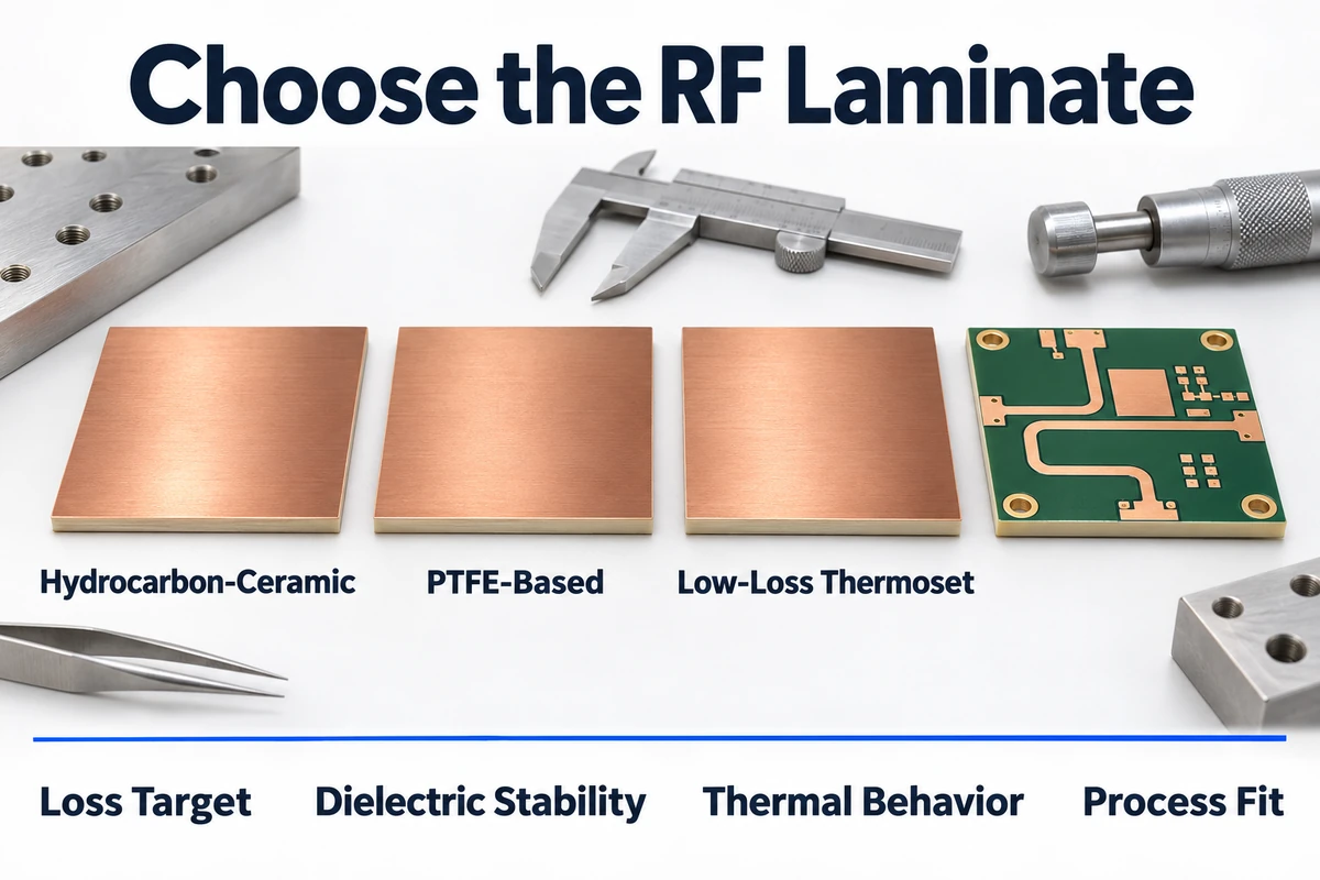
Selecting an RF substrate requires balancing dielectric constant (Dk), dissipation factor (Df), thermal expansion (CTE), and manufacturing complexity. The table below compares widely specified commercial high-frequency laminates based on published manufacturer technical datasheets.
| Laminate Grade | Manufacturer & Material Class | Process Dk | Design Dk | Dissipation Factor (Df) | Z-Axis CTE | Primary Processing Considerations | Common Engineering Applications |
|---|---|---|---|---|---|---|---|
| Rogers RO4350B | Rogers Corp. (Hydrocarbon / Ceramic) | 3.48 ± 0.05 (@ 10 GHz) | 3.66 (@ 8–40 GHz) | 0.0037 (@ 10 GHz) | 31 ppm/°C | Standard FR-4 processing line compatible; no plasma desmear required | Commercial RF, cellular base stations, automotive sensors, and FR-4 hybrid multilayers |
| Rogers RO4003C | Rogers Corp. (Hydrocarbon / Ceramic) | 3.38 ± 0.05 (@ 10 GHz) | 3.55 (@ 8–40 GHz) | 0.0027 (@ 10 GHz) | 46 ppm/°C | Lower dielectric loss than RO4350B; requires lead-free processing review | Microwave communications, radar transceivers, and satellite LNBs |
| Rogers RO3003 | Rogers Corp. (Ceramic-filled PTFE) | 3.00 ± 0.04 (@ 10 GHz) | 3.00 (@ 8–40 GHz) | 0.0010 (@ 10 GHz) | 25 ppm/°C | Excellent Dk stability vs. temperature; requires plasma or sodium-etch hole conditioning | 77 GHz automotive radar patch antennas, mmWave sensors, and high-frequency wireless |
| Rogers RO3010 | Rogers Corp. (Ceramic-filled PTFE) | 10.2 ± 0.30 (@ 10 GHz) | 11.20 (@ 8–40 GHz) | 0.0022 (@ 10 GHz) | 16 ppm/°C | High dielectric constant enables circuit miniaturization; soft PTFE matrix | Compact RF filters, couplers, patch antennas, and satellite receiver front-ends |
| Rogers RT/duroid 5880 | Rogers Corp. (Glass Microfiber PTFE) | 2.20 ± 0.02 (@ 10 GHz) | 2.20 (@ 8–40 GHz) | 0.0009 (@ 10 GHz) | ~135 ppm/°C | Ultra-low dielectric loss; soft substrate requires careful drilling parameters | Aerospace, missile guidance systems, military radar, and high-frequency antenna feeds |
| Taconic RF-35 | Taconic / AGC (Organic-ceramic PTFE) | 3.50 ± 0.05 (@ 1.9 GHz) | ~3.50 | 0.0018 (@ 1.9 GHz) | ~64 ppm/°C | Balanced peel strength and low moisture absorption (<0.02%) | Power amplifiers, filters, transceivers, and commercial antenna arrays |
| Isola Astra MT77 | Isola Group (Low-loss Thermoset) | 3.00 (@ 2–20 GHz) | ~3.00 | 0.0017 (@ 2–20 GHz) | 45 ppm/°C | High-Tg thermoset compatible with standard multilayer and sequential lamination | 5G infrastructure, satellite communications, and high-speed mixed-signal backplanes |
How to Ensure Prototype-to-Production Continuity (A 4-Point Transfer Framework)
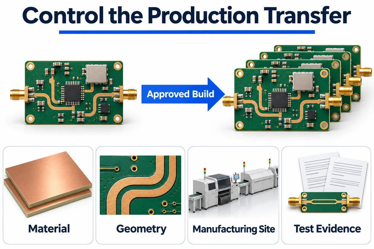
The central risk when transitioning an RF PCB design from NPI prototyping to volume production is electrical and mechanical drift. A prototype that functions within specification can fail in production if laminate parameters, copper morphology, or test tolerances vary across build lots.
Hardware engineering teams can use the following Four-Control RF Transfer Framework as an internal checklist to ensure manufacturing consistency:
1. Differentiate Design Dk from Process Dk and Lock the Substrate Callout
High-frequency material datasheets frequently report two distinct dielectric constant values:
- Process Dk: A quality-control baseline measured using clamped stripline test fixtures (e.g., 3.48 for Rogers RO4350B at 10 GHz per IPC-TM-650).
- Design Dk: The effective dielectric constant experienced by microstrip or coplanar transmission lines in actual fabricated circuits (e.g., 3.66 for RO4350B across 8–40 GHz).
Ensure CAM and signal integrity engineers use the correct frequency-dependent Design Dk during impedance modeling. Furthermore, specify the exact laminate brand, grade, and prepreg type on the fabrication drawing rather than generic designations like “equivalent RF laminate.” Alternates with nominally identical Dk can exhibit differing resin flow, dissipation factor, or thermal expansion characteristics that alter circuit performance.
2. Specify Copper Foil Roughness and Etch Compensation Rules
At microwave frequencies, current flow is confined to a thin layer near the conductor surface due to the skin effect. Microscopic roughness at the copper-to-dielectric interface increases electrical path length and conductor insertion loss:
- Foil Profile Specification: Identify whether the design requires Standard Electrodeposited (ED), Reverse-Treated (RTF), Very-Low-Profile (VLP/HVLP), or Rolled Annealed (RA) copper foil on RF layers.
- Etch Profile & Tolerances: Microwave filters, coupled lines, and millimeter-wave patch antennas are sensitive to conductor width variations and trapezoidal trace cross-sections. Define critical trace width tolerances and confirm the fabricator’s CAM etch compensation rules during technical review.
3. Control Via Stub Length, Hole Preparation, and Solder Mask Relief
Multilayer RF signal paths require careful attention to vertical via transitions and surface coatings:
- Via Stub Minimization: Unused portions of plated-through-hole barrels create open-ended stubs that cause signal reflections at higher frequencies. Where applicable, specify controlled-depth backdrilling or blind microvias, and state the allowable remaining stub length.
- PTFE Hole Wall Conditioning: Ceramic-filled and pure PTFE substrates require specialized hole-wall preparation (such as plasma desmear or sodium-etch chemical treatment) to ensure copper plating adhesion and prevent barrel separation under thermal cycling.
- Solder Mask Over High-Frequency Nets: Solder mask has higher dielectric loss (Df ~0.02) and less uniform thickness than specialized RF substrates. Keep critical RF traces, matching networks, and antenna elements solder-mask relieved, and select surface finishes (such as Immersion Silver or ENEPIG) based on insertion loss and wire-bonding requirements.
4. Standardize Test Coupon Verification and Transfer Protocols
Controlled impedance on a purchase order must be paired with defined verification deliverables:
- Test Coupon Alignment: Specify coupon requirements (such as single-ended, differential, or coplanar test structures) that reflect the board’s critical transmission line geometry.
- Inspection Deliverables: Determine the required verification package, which may include Time-Domain Reflectometry (TDR) reports, cross-sectional microsection analysis (confirming dielectric thickness and copper plating), or project-specific S-parameter Vector Network Analyzer (VNA) sweeps.
- Production Site Continuity: When a supplier operates multiple manufacturing plants, include a site-lock requirement stating that production builds must remain at the qualified facility or undergo an approved First Article Inspection (FAI) before volume release.
RF PCB & PCBA RFQ Checklist for Hardware Teams
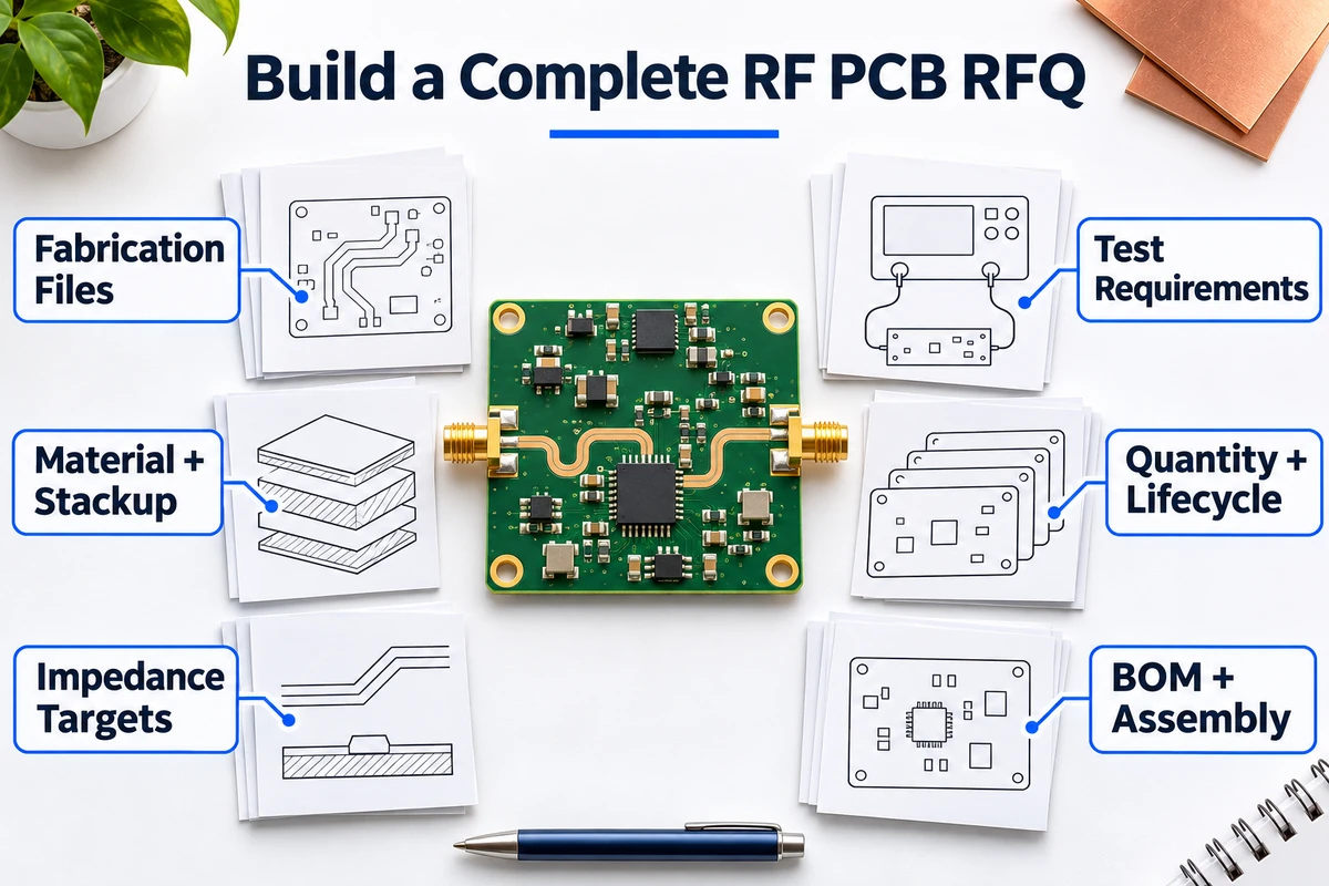
Providing a clear, comprehensive technical package ensures all candidate manufacturers quote against identical engineering baselines.
| RFQ Package Item | Technical Information to Provide | Engineering Purpose |
|---|---|---|
| Design Data & Master Drawing | Gerber X2, ODB++, or IPC-2581 files, NC drill files, and a controlled PDF master drawing revision | Establishes an unambiguous design baseline across all quoting suppliers |
| Laminate & Bondply Callout | Exact laminate brand and grade, dielectric thickness, bondply type, and approved alternate policy | Prevents unverified substrate substitutions that shift electrical parameters |
| Finished Copper & Foil Type | Layer copper weights (e.g., 0.5 oz, 1 oz) and preferred foil profile (ED, RTF, VLP, or Rolled) | Controls conductor loss and skin-effect attenuation across microwave traces |
| Impedance Targets & Tolerances | Target impedance values, reference planes, line geometry, and required tolerance (e.g., ±10% or ±5%) | Makes controlled impedance verifiable against defined coupon structures |
| Via & Backdrill Rules | Maximum allowable backdrill stub length, via fill types (IPC-4761), and microvia aspect ratios | Reduces via reflections and prevents solder wicking on thermal ground pads |
| Surface Finish & Mask Relief | ENIG, Immersion Silver, ENEPIG, or selective gold, with solder mask relief callouts for RF lines | Avoids dielectric loss from solder mask and matches component assembly needs |
| Special Mechanical Features | Depth-milled cavities, edge plating, castellations, copper coins, or metal backing requirements | Clarifies required precision machining, plating tanks, or carrier bonding |
| Inspection & Quality Data | Required TDR reports, microsections, laminate Certificates of Conformance, or S-parameter data | Aligns documentation costs and quality assurance expectations upfront |
| Assembly Documentation | Complete BOM, centroid pick-and-place data, special component handling, and X-ray inspection rules | Enables accurate turnkey assembly quoting and thermal reflow profile planning |
| Volume & Lifecycle Schedule | Prototype quantities, expected pilot run, estimated annual volume, and facility transfer terms | Evaluates supplier capacity across the complete prototype-to-production lifecycle |
FAQs About RF PCB Manufacturers
Can One Manufacturer Build Both RF Prototypes and Production Boards?
Yes, several manufacturers support both rapid prototyping and production builds. The key engineering requirement is confirming that production runs will preserve the same laminate material source, stackup architecture, etch compensation, and test methods established during the prototype phase. When volume production is allocated to a different facility or line, hardware teams should require a formal First Article Inspection (FAI) and test coupon verification before approving volume shipments.
Should RF Prototypes and Production Boards Use the Same Stackup?
They should normally use an electrically equivalent, engineering-approved stackup. While minor adjustments may sometimes be considered for panel utilization or material availability, any change to dielectric thickness, laminate grade, copper roughness, or prepreg type can alter trace impedance, insertion loss, and resonant frequencies. All proposed stackup modifications should be reviewed with field-solver simulations and verified on test coupons.
When Is a Hybrid RF/FR-4 Stackup Preferable to an All-RF Board?
A hybrid stackup—which pairs outer high-frequency laminates (such as Rogers RO4350B or RO3003) with inner High-Tg FR-4 cores and prepregs for digital control and power distribution—is commonly used in multilayer designs where RF routing is confined to specific layers. Hybrid constructions significantly reduce laminate material costs and enhance mechanical rigidity, provided the fabricator manages lamination press cycles and matches coefficient of thermal expansion (CTE) characteristics to prevent board warpage.
What Test Deliverables Should Be Requested for an RF PCB Build?
Standard deliverables include panelized Time-Domain Reflectometry (TDR) impedance coupon reports, cross-sectional microsection analysis (verifying dielectric thickness, copper plating, and etch factors), and laminate manufacturer Certificates of Conformance (CoC). For high-frequency microwave or radar applications, projects may also specify Vector Network Analyzer (VNA) S-parameter measurements (S11 return loss and S21 insertion loss) on defined test transmission lines.
Which Surface Finish Is Best Suited for High-Frequency PCBs?
Immersion Silver is widely used for high-frequency and microwave circuits because it provides a smooth, planar surface with low conductor loss. ENEPIG (Electroless Nickel Electroless Palladium Immersion Gold) is favored for mixed-technology boards requiring both SMT soldering and gold or aluminum wire bonding. ENIG (Electroless Nickel Immersion Gold) remains common for many commercial designs up to 10–20 GHz, though engineers should evaluate the magnetic properties and skin-effect losses of the electroless nickel layer at higher microwave frequencies.
How Should Hardware Teams Choose Between US, European, and Asian Manufacturers?
Supplier selection should be guided by regulatory, speed, and cost requirements: US manufacturers (TTM, Sierra Circuits, Summit, AdvancedPCB, ASC) are well-suited for projects requiring domestic defense/aerospace compliance or close geographic collaboration during early-stage prototyping. European manufacturers (Cistelaier, Schweizer Electronic) are practical for European aerospace, defense, and automotive Tier-1 programs requiring regional supply chains and multi-material qualifications. China-based integrated manufacturers like OrinewPCB fit commercial, telecommunications, and industrial projects that benefit from competitive multilayer fabrication, stocked high-frequency laminates, and integrated turnkey PCB assembly in a single sourcing relationship.
Sources
This shortlist was compiled from public manufacturer documentation, official capability sheets, and engineering reference materials reviewed in November 2026. Companies were selected based on their published capabilities in processing high-frequency laminates, controlled-impedance fabrication, and prototype-to-production lifecycle support.
Manufacturer capability pages serve as primary sources for offered processes, but published specifications represent general capabilities that must be verified against project-specific designs. Readers should confirm material availability, process tolerances, and test deliverables directly with candidate suppliers during technical RFQ reviews.
RF PCB PROTOTYPE TO PRODUCTION
Move your RF design from prototype to controlled production
OrinewPCB supports high-frequency PCB fabrication and turnkey assembly discussions for RF, microwave, and high-speed mixed-signal designs. Hardware teams can submit CAD data, proposed stackups, impedance requirements, and assembly specifications for engineering DFM review and controlled-impedance modeling.
- High-frequency PCB fabrication
- Stocked Rogers, Taconic & PTFE laminates
- Hybrid RF/FR-4 stackup modeling
- Turnkey SMT assembly & TDR test options
Get Quote Free