DIP and wave soldering in modern PCBA: an engineering guide
Learn when DIP through-hole assembly and wave soldering are the right PCBA choices, how to design for them, and how to control reliable solder-joint quality.
Get Your PCB Quote!
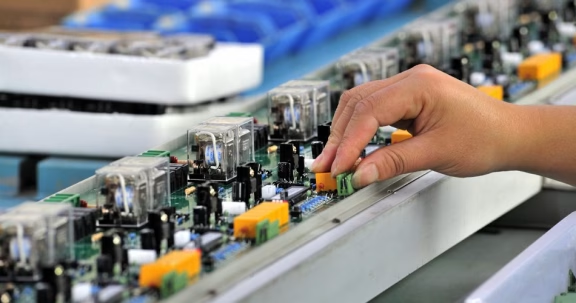
Table of Contents
- Key takeaways
- What DIP plug-in soldering means in a current production line
- When through-hole assembly is the engineering choice
- Choose the soldering route before layout is frozen
- Design for a solderable through-hole joint
- Control the wave, not just the solder pot
- Build an inspection plan around failure modes
- Common defects and the right first question
- How DIP fits alongside SMT in a modern PCBA flow
- A practical release checklist for THT builds
- Frequently asked questions
- Sources and related reading
Table of Contents
- Key takeaways
- What DIP plug-in soldering means in a current production line
- When through-hole assembly is the engineering choice
- Choose the soldering route before layout is frozen
- Design for a solderable through-hole joint
- Control the wave, not just the solder pot
- Build an inspection plan around failure modes
- Common defects and the right first question
- How DIP fits alongside SMT in a modern PCBA flow
- A practical release checklist for THT builds
- Frequently asked questions
- Sources and related reading
DIP plug-in soldering remains a production process, not a legacy exception. In modern PCBA, through-hole technology (THT) is often the deliberate choice for connectors, relays, transformers, large electrolytic capacitors, power devices, switches, and any part whose load path is not well served by a surface-mount termination. The engineering question is not whether SMT has replaced THT. It is whether the component, board layout, and production volume can make a repeatable through-hole joint.
For a production build, that answer depends on more than selecting a wave solder machine. Lead geometry, hole and pad design, board mass, flux coverage, preheat, conveyor settings, solder alloy control, and inspection evidence all work together. IPC J-STD-001J describes process, material, and acceptance requirements for soldered electronic assemblies, while IPC-A-610J is used for post-assembly acceptability. IPC explains the distinction between the two standards.
Key takeaways
- Use THT where retention, connector mating force, current handling, thermal mass, or component availability justifies a plated-through-hole interconnect.
- Treat wave soldering as a controlled thermal process. A visually shiny joint alone is not proof that the barrel filled or that the process is stable.
- Decide early whether the board is suitable for wave, selective soldering, pin-in-paste reflow, or hand soldering. This is a layout and DFM decision, not a last-minute routing change.
- Request an agreed inspection plan before production, especially for high-reliability assemblies and concealed connector barrels.
What DIP plug-in soldering means in a current production line
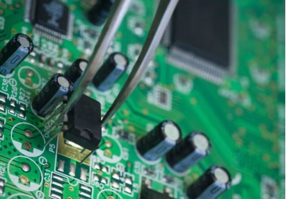
DIP originally describes a dual in-line package, but production teams often use “DIP” to mean the broader through-hole insertion and soldering stage. Components are inserted into plated holes, their leads are retained or formed as required, and solder creates the electrical and mechanical connection between lead, plated barrel, and pad.
That last point matters. A connector can survive an initial functional test even when barrel fill, wetting, or lead protrusion is inconsistent. The risk appears later as intermittent contact, mechanical damage during mating, or difficult rework. The appropriate acceptance class and product requirements must be agreed with the customer; “IPC compliant” by itself is not a complete build instruction.
When through-hole assembly is the engineering choice
THT earns its board area when the joint must do more than carry a low-force electrical signal. Typical triggers include:
- I/O connectors exposed to repeated insertion, removal, or cable strain.
- Relays, transformers, inductors, and large capacitors with significant mass or height.
- Power semiconductors and terminals that need robust leads or mechanical support.
- Components whose approved package is only available in through-hole form.
- Serviceable products where a technician must be able to inspect or replace a component.
This is not a claim that every large or high-current part must be through-hole. Some designs use surface-mount power packages successfully. The practical rule is to model the mechanical load and service environment, then select the package and assembly method together. If a connector is taking cable load, do not assume its signal pins are the retention system; use locating posts, mounting hardware, or a connector design rated for that load.
| Project condition | Engineering implication | Questions to settle before release |
| Connector or switch sees repeated force | Joint needs mechanical support as well as electrical continuity | Are locating posts, mounting tabs, or hardware specified? What load reaches the solder joints? |
| Mixed SMT and THT board | Keep-outs and component orientation influence solder access | Can bottom-side SMT parts tolerate the selected solder process? |
| Low-volume or high-mix build | Changeover and fixture complexity may outweigh wave efficiency | Would selective or hand soldering give better control? |
| High-volume repeat build | Process window and repeatable fixturing become critical | Is the panel, pallet, and inspection plan validated on a pilot run? |
Choose the soldering route before layout is frozen
“Through-hole” does not automatically mean “wave soldered.” The correct process is chosen from the assembly geometry, thermal constraints, access, and expected volume.
Wave soldering
Wave soldering is efficient when many compatible through-hole joints can pass over a controlled solder wave in one operation. It is particularly useful for repeatable production, but it requires good layout discipline. Bottom-side SMT components, connectors with traps, large copper planes, and uneven thermal mass can narrow the usable process window.
Selective soldering
Selective soldering applies solder locally, making it useful where a full wave would expose nearby parts or where only a small number of THT joints exist. It can reduce the need for wave pallets, but it still needs validated access, nozzle clearance, and thermal profiling.
Pin-in-paste reflow and hand soldering
Pin-in-paste can work for selected components when paste volume, lead geometry, and reflow profile are engineered for the joint. Hand soldering is often appropriate for prototypes, rework, and low-volume exceptions, but it should use documented workmanship criteria rather than relying on individual technique. IPC’s J-STD-001 program explicitly includes through-hole, machine, and reflow soldering requirements.
Design for a solderable through-hole joint
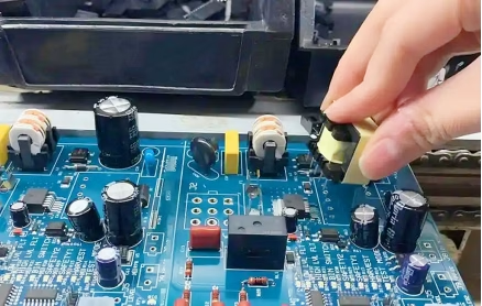
The most expensive wave-solder defect is often created in CAD. A production review should look beyond nominal hole size and ask how the board will move through the process.
- Confirm finished hole, lead diameter, and lead-to-hole clearance against the approved component drawing and fabrication capability.
- Provide adequate annular ring and copper connection for the product class and current path.
- Keep heat-sinking copper, large grounded barrels, and heavy terminals visible to the process engineer. They may need a different thermal strategy, not simply more dwell time.
- Orient compatible components consistently where possible, and reserve access for pallets, selective nozzles, probes, and visual inspection.
- Identify bottom-side SMT components that could shadow a THT joint or see an unacceptable thermal exposure.
- Include polarity, reference designators, insertion notes, and any lead-forming requirements in the assembly documentation.
One recurrent DFM issue is treating a connector footprint as only an electrical symbol. On real builds, its shell tabs, pegs, mating direction, board edge clearance, and inspection access determine whether the joint is manufacturable. That is why PCBAndAssembly reviews the BOM, Gerber data, centroid data, and assembly drawing as one package rather than independently.

Control the wave, not just the solder pot
A wave line is a system: flux application, preheat, conveyor movement, contact with the solder wave, cooling, and maintenance. Changing one setting to fix an apparent defect can create another defect elsewhere. For example, insufficient flux coverage, excessive conveyor speed, contamination, and unsuitable preheat can all contribute to bridging in a vendor technical guide; treat those values as product-and-flux-specific starting points, not universal settings. AIM Solder’s flux data sheet is a useful example of the process variables that must be documented.
The process record should therefore include the actual alloy and flux, flux density or control method, profile measurements for the board family, conveyor configuration, solder-pot maintenance, and the defined inspection response when a limit is missed. A profile from a lightweight test coupon is not automatically valid for a finished board carrying a transformer, large connectors, or heavy copper.
Build an inspection plan around failure modes
Inspection should answer a defined risk question, not merely create a final checkpoint. Visual inspection can identify bridges, insufficient wetting, solder balls, damaged components, polarity mistakes, and lead condition. Functional testing proves that the assembly operates under the test conditions. Neither necessarily proves the other.
For barrels or joints that cannot be assessed reliably from one side, agree on the evidence before the first production lot. Depending on the product, that can mean process qualification, sample cross-sections, x-ray, electrical test, or a controlled first-article review. NASA has documented the importance of confirming that solder wets the full through-hole around connector pins, especially when the joint is not directly visible. NASA’s technical brief on fully soldered through holes illustrates the underlying concern.
Common defects and the right first question
| Observed condition | Do not assume | Start by checking |
| Bridging between leads | That solder temperature alone caused it | Flux coverage, lead spacing, board orientation, conveyor settings, contamination, and wave stability |
| Insufficient hole fill or poor wetting | That more solder contact time is always safe | Board/component solderability, thermal mass, preheat, flux activity, and hole/lead geometry |
| Icicles or excess solder | That the defect is only cosmetic | Wave condition, withdrawal geometry, lead length, solderability, and the electrical clearance risk |
| Lifted pad or damaged laminate | That rework can restore the original reliability | Rework temperature control, dwell time, copper adhesion, and whether the board needs engineering disposition |
The useful corrective-action habit is to trace a defect back through material, design, and process evidence. Repeatedly adjusting the solder pot without checking flux delivery or hole geometry can hide the real cause until the next lot.
How DIP fits alongside SMT in a modern PCBA flow
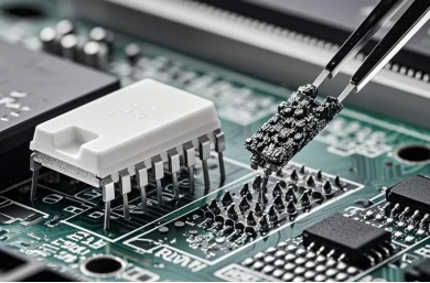
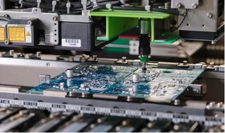
Most mixed-technology boards use SMT for density and automated placement, then add THT where mechanical or electrical needs justify it. The integration point is the process plan: which side is reflowed first, whether the board needs a pallet, what components need post-reflow insertion, and how the assembly will be tested and depanelized.
For a broader view of surface-mount production, see our SMT assembly service. For test strategy, the PCB assembly testing guide explains why inspection and functional evidence should be selected by product risk.
A practical release checklist for THT builds
- Package the Gerber files, BOM, assembly drawing, centroid data, and revision-controlled component substitutions together.
- Mark every through-hole component that has polarity, lead-forming, insertion-height, torque, or hardware requirements.
- State the required assembly standard revision and acceptance class in the purchase documentation.
- Tell the manufacturer which joints are safety-, load-, or reliability-critical, and agree how they will be verified.
- Ask whether wave, selective, pin-in-paste, or hand soldering is planned for each THT group before production begins.
- Use a pilot build to validate the panel, tooling, profile, inspection points, and functional-test coverage before scaling.
PCBAndAssembly can review these inputs during a PCB assembly quote and DFM review. The aim is not to force every through-hole part through a wave. It is to choose the soldering route that gives the intended joint a stable, inspectable production process.
Frequently asked questions
Is DIP plug-in soldering the same as wave soldering?
No. DIP plug-in soldering describes the insertion and soldering of through-hole components. Wave soldering is one automated method for forming those joints. Selective soldering, pin-in-paste reflow, and controlled hand soldering may be better choices for a particular layout or volume.
Can SMT and THT components be used on the same PCB?
Yes. Mixed-technology assembly is common. The important decision is the sequence and thermal exposure: bottom-side parts, wave keep-outs, pallets, component orientation, and test access should be reviewed together.
What should be specified for a critical connector joint?
Provide the exact component and footprint, mating/load expectations, required assembly standard and class, any barrel-fill or inspection requirement, and the test evidence expected. If the joint cannot be judged visually, agree on a process-validation method before the build.
When is selective soldering preferable to wave soldering?
Selective soldering is often preferable when a board has only a few THT joints, sensitive bottom-side SMT parts, or geometry that makes a full-wave pass difficult. The decision should be based on accessibility, repeatability, tooling, and production volume.
Sources and related reading
Get Quote Free