Modern PCB Assembly: SMT, Through-Hole & Emerging Tech
Modern PCB assembly is more than placing components on a board. It is a connected manufacturing process that links design data, component sourcing, SMT and THT production, inspection, testing, traceability, and engineering feedback.
Get Your PCB Quote!
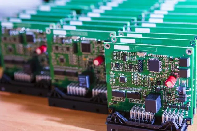
Table of Contents
- Devre Kartı Düzeneği Nedir?
- Baskılı Devre Kartları ve Rolleri
- Modern PCB montaj iş akışı
- SMT, THT ve karma teknoloji montajı
- Mecliste Karşılaşılan Zorluklar
- Anlaşılması gereken yeni teknolojiler
- Otomasyon neleri değiştiriyor ve neleri değiştirmiyor?
- Özel Üretim ve Seri Üretim
- PCBAndAssembly: Profesyonel PCB Montajı İçin Ortağınız
- Sıkça Sorulan Sorular
- Sonuç
Table of Contents
- Devre Kartı Düzeneği Nedir?
- Baskılı Devre Kartları ve Rolleri
- Modern PCB montaj iş akışı
- SMT, THT ve karma teknoloji montajı
- Mecliste Karşılaşılan Zorluklar
- Anlaşılması gereken yeni teknolojiler
- Otomasyon neleri değiştiriyor ve neleri değiştirmiyor?
- Özel Üretim ve Seri Üretim
- PCBAndAssembly: Profesyonel PCB Montajı İçin Ortağınız
- Sıkça Sorulan Sorular
- Sonuç
Electronics have changed from being bulky components and simple circuits. The gadgets today are slim, powerful, and ever decreasing in size. With circuit card assembly forming the basis of all such innovations, that is the crucial process which breathes life into modern electronics.
From the smartphone all the way to aerospace technology, circuit boards make it all work. How are they assembled, exactly? Let us now witness the manufacturing and assembly of the building blocks of modern technology.
What is Circuit Card Assembly?
Circuit card assembly (CCA) is the process of attaching electronic components to a printed circuit board (PCB). The board itself is made of non-conductive material — typically FR-4 fiberglass — with conductive copper pathways etched onto its surface. These pathways connect components to form a working electronic circuit.
CCA is not simply “attaching parts.” It requires precision planning, clean execution, and rigorous validation. The same assembly process that powers a smartwatch must also be reliable enough for a server farm running 24/7 or a medical device that monitors a patient’s vital signs.
Key Distinction: CCA vs. PCBA
| Term | Meaning | Scope |
| CCA (Circuit Card Assembly) | The populated board with all components installed | Focus on the assembled circuit card itself |
| PCBA (Printed Circuit Board Assembly) | The result of PCB fabrication + component assembly | Broader term encompassing the full build |
| PCB (bare board) | The unpopulated board with copper traces only | The substrate before assembly |
In practice, the terms CCA and PCBA are often used interchangeably, though PCBA is more common in the industry.
Printed Circuit Boards and Their Role
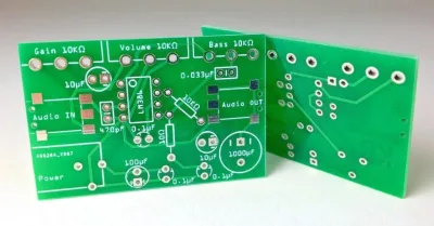
PCBA is an acronym for printed circuit board assembly, which refers to the result of a board being built and all components being installed on top of it. The actual base board is referred to as a PCB, upon which all parts are placed.
What distinguishes one board from another is its intricacy. Some PCB designs are single-sided with few components on them. Some are multilayer designs, intricately routed for faster speeds and higher power.
PCB Complexity Levels
| Type | Layer Count | Typical Applications | Relative Cost |
| Single-sided | 1 | Simple consumer electronics, LED lighting | Low |
| Double-sided | 2 | Power supplies, automotive ECUs | Low-Moderate |
| Multilayer | 4-8 | Computer motherboards, industrial controllers | Moderate |
| High-density (HDI) | 6-20+ | Smartphones, tablets, 5G modules | High |
| Heavy copper | 4-10+ | Power converters, EV battery management | High |
Designing a PCB requires careful consideration of heat dissipation, electrical noise (EMI), signal integrity, and spatial constraints. A poorly designed board cannot be saved by assembly — the decisions made at the PCB design stage determine whether the final product succeeds or fails.
The modern PCB assembly workflow
1. Start with controlled design data
Automation begins before the board reaches the factory. A typical production package includes:
- Gerber, ODB++, or IPC-2581 fabrication data
- BOM with manufacturer part numbers, reference designators, quantities, and approved alternates
- Pick-and-place data with coordinates, rotation, side, and origin
- Assembly drawings with polarity, orientation, no-populate areas, and mechanical keep-outs
- Test-point map, programming instructions, and functional-test limits
- Revision numbers shared across the PCB data, BOM, drawings, firmware, and test procedure
The most common automation mistake is allowing different systems to use different revisions. A placement machine can execute a wrong file perfectly. Before programming the line, the manufacturer should compare the BOM, centroid file, assembly drawing, and PCB revision as one controlled package.
Engineering note: A DRC-clean layout is not automatically assembly-ready. DRC may confirm spacing and connectivity, but it usually does not tell you whether a test probe can reach a pad, whether a connector collides with a fixture, or whether a large copper area will create an uneven reflow profile. DFM and DFA close that gap.
2. Review DFM, DFA, and test access
The DFM/DFA review should cover more than line-width rules. For modern PCB assembly, ask the manufacturing engineer to review:
- Fiducials and board registration
- Panel rails, tooling holes, and depanelization method
- Component spacing around fine-pitch packages and connectors
- Stencil aperture design and solder-paste volume
- Polarity marks and component orientation
- Thermal balance across the reflow profile
- Moisture-sensitive components and handling requirements
- Test-point access for power, programming, communication, and critical nets
- Mechanical support for tall, heavy, or high-insertion-force parts
- Coating, cleaning, programming, and final-test keep-outs
The point is not to make every design look the same. It is to identify which design choices affect yield, rework, test coverage, lead time, or field reliability before tooling and component purchases are committed.
3. Source, inspect, and prepare components
Turnkey assembly requires more than buying the correct quantity. The manufacturer must control manufacturer part numbers, approved alternates, packaging, date or lot information where required, and moisture-sensitive handling.
Incoming inspection can include quantity verification, label and part-number checks, package inspection, and sampling against the customer’s requirements. For products with long service lives or regulatory obligations, traceability should connect the component lot to the assembled board’s serial number or production record.
IPC-1782 defines minimum requirements for manufacturing and supply-chain traceability based on perceived risk and applies to printed board assemblies, components, equipment, and related processes. The practical question is not whether a factory has “traceability” as a slogan. Ask what is recorded, how long it is retained, and whether the record can be retrieved for a specific board or lot.
4. Print solder paste and measure it with SPI
The SMT line begins with stencil printing. A printer deposits solder paste onto the pads, and the stencil controls where the paste goes. Aperture size, stencil thickness, paste chemistry, board support, alignment, and print parameters all affect the result.
3D solder-paste inspection measures deposited paste volume, height, area, and position. This is valuable because it detects a printing problem before components cover the pads. When SPI is connected to the printer, the process can be adjusted using measured data rather than relying only on end-of-line inspection.
Do not treat SPI as a replacement for AOI. SPI evaluates the paste deposit before placement. AOI evaluates the assembled board after soldering. They control different points in the process.
5. Place SMT components with a controlled recipe
Pick-and-place machines use feeders, nozzles, vision systems, fiducials, and placement programs to install surface-mount components. SMT supports small packages, high component density, double-sided assembly, and repeatable production at scale.
The machine is only as reliable as its recipe and material controls. A modern line should control feeder setup, component verification, nozzle maintenance, placement offsets, and program revision. For a first article, the manufacturer should review placement exceptions rather than silently correcting them on the machine.
Common SMT risks include:
- Incorrect component loaded into a feeder
- Wrong rotation or polarity
- Tombstoning caused by pad or thermal imbalance
- Solder bridging on fine-pitch parts
- Missing or shifted components
- Warpage or support problems on large boards
- Moisture-related package damage during reflow
6. Reflow solder with a measured profile
Reflow soldering melts the paste and forms the electrical and mechanical joints. The profile must suit the solder alloy, component temperature limits, board thickness, copper distribution, and assembly side.
A profile copied from another product is not automatically correct. A heavy-copper board, a large ground plane, and a small high-density region can heat differently in the same oven. The production record should identify the approved profile and any product-specific qualification or profile verification.
For soldered assemblies, IPC J-STD-001J addresses materials, methods, and acceptance criteria for producing soldered electrical and electronic assemblies. IPC-A-610J is used for post-assembly visual acceptability. IPC explains that the two standards are commonly used together, while IPC-A-610J itself is not a complete X-ray or cross-section specification.
7. Inspect the assembled SMT board
AOI checks visible conditions such as component presence, placement, orientation, polarity, solder coverage, and selected solder-joint features. 3D AOI adds height and shape information that can improve detection of lifted leads, insufficient solder, and component displacement.
X-ray is useful when a connection is hidden from the camera. BGA, QFN, bottom-terminated components, and some connector or through-hole joints may require X-ray or another defined inspection method. The need depends on package geometry, product risk, customer requirements, and the agreed acceptance plan.
The correct question is not “Do you have AOI?” It is:
Which defects can your AOI detect on this design, which areas need X-ray, and how are false calls and escapes handled?
For a deeper explanation of visual inspection, see the guide to automated optical inspection in PCB assembly.
SMT, THT, and mixed-technology assembly
SMT and THT are not competing technologies in every design. Modern products commonly combine them.
| Method | Best fit | Main trade-off |
| SMT assembly | Dense logic, memory, sensors, RF parts, small passives, and automated high-mix production | Requires careful stencil, placement, reflow, and fine-pitch inspection |
| THT assembly | Connectors, transformers, relays, large capacitors, switches, and parts exposed to mechanical load | Uses drilled holes and requires insertion plus wave, selective, or manual soldering |
| Selective soldering | A defined group of THT joints on a mixed-technology board | Needs nozzle, pallet, thermal, and keep-out planning |
| Wave soldering | Suitable groups of through-hole joints on a prepared board | May expose nearby SMT components to heat and solder contact |
| Press-fit | Approved connectors or pins where the mechanical and electrical specification supports it | Requires controlled hole size, insertion force, and inspection |
| Manual soldering | Prototype changes, unusual parts, repair, or low-volume operations | More operator-dependent and needs clear work instructions |
When THT is still the right answer
THT is not obsolete simply because SMT is faster. A connector that will be plugged and unplugged repeatedly may need the mechanical retention of a through-hole design. A transformer or relay may need lead spacing and body support that a surface-mount package cannot provide.
The decision should follow the load path. Ask what force the component will experience, whether the board has a supporting enclosure or bracket, how it will be soldered, and how the joint will be inspected. THT is often strongest when the mechanical design, PCB holes, component leads, solder process, and enclosure are reviewed together.
Challenges Faced in Assembly
Every production line faces unique challenges. Miniaturisation is one of the defining aces of circuit board assembly. As the device will become smaller, the components will too.
0201 (0.6mm x 0.3mm), 01005 (0.4mm x 0.2mm), and even 008004 packages are now common. These require:
- Sub-micron placement accuracy from pick-and-place machines
- Laser-cut stencils with precise aperture geometry
- Optimized solder paste formulations for consistent release
- High-resolution 3D AOI for defect detection
Another fairly common problem faced would be heat. During reflow soldering, the board goes through high-temperature stages, and if it is a little hard for the entire process, some components will suffer damages and defects will be detected in soldering.
During reflow soldering, boards pass through high-temperature zones. Thermal issues include:
- Component damage: Heat-sensitive parts may exceed their rated temperature
- Board warpage: Uneven heating causes FR-4 to bend, affecting solder joint quality
- Thermal shadowing: Large components block heat from smaller parts behind them
- Head-in-pillow defects: BGA balls fail to coalesce with paste due to temperature differences
Solutions include thermal profiling (using thermocouples on actual boards), zone-controlled reflow ovens, and nitrogen atmosphere for better heat transfer.
Electromagnetic interferences (EMI) are also becoming a great concern. Poor design or assembly can introduce signal noise. This affects performance, especially in high-speed circuits.
Common EMI issues include:
- Improper ground plane connections
- Insufficient decoupling capacitor placement
- Long signal return paths
- Crosstalk between adjacent traces
New technologies worth understanding
Connected factory data with IPC-CFX
IPC-2591 Connected Factory Exchange, or CFX, defines communication between manufacturing processes and associated host systems. IPC describes it as an open standard for exchanging information across automated, semiautomated, and manual assembly processes.
CFX is useful when the factory needs to connect printers, placement machines, reflow, inspection, test, material systems, and production software without building a separate custom interface for every machine. IPC’s 2025 CFX 2.0 release added capabilities for hand soldering and wave soldering, richer placement information, recipe changes, and traceability of board differences.
That does not mean every factory has a complete smart-factory implementation. When evaluating a supplier, ask which equipment is connected, what data is captured, whether the data is tied to a board serial number, and what the customer actually receives.
AI-assisted inspection
Machine-vision inspection increasingly uses software classification and data analysis to reduce false calls and highlight unusual patterns. The useful application is not “AI guarantees zero defects.” It is helping engineers prioritize defects, tune inspection libraries, and identify drift across lots.
AI should remain inside a controlled quality process. The supplier still needs approved inspection criteria, a human disposition process, version-controlled inspection programs, and an escalation path for new or ambiguous defects.
3D SPI and 3D AOI
Three-dimensional measurement adds height and volume information to traditional image-based inspection. That can be useful for paste volume, component lift, lead geometry, and solder-joint shape. It is especially valuable when the same board contains a mix of large passive components, fine-pitch packages, and connectors.
The benefit depends on recipe quality and the defect library. More dimensions do not automatically mean better coverage if the program is poorly tuned or the reference data is incomplete.
Advanced soldering and dispensing
Selective soldering, solder jetting, laser-assisted soldering, dispensing, and controlled manual operations can help with mixed-technology boards, thermal-sensitive areas, repair, and low-volume variation. They are process choices, not universal upgrades.
For example, selective soldering may reduce unnecessary heat exposure compared with wave soldering, but it requires correct nozzle access, pallet design, component keep-outs, and thermal qualification. A supplier should recommend the process based on the actual board, not merely list every available machine.
Advanced packages and board-level integration
Package-on-package, micro-BGA, QFN, bottom-terminated components, embedded components, chip-on-board, rigid-flex, and high-density interconnects can reduce size or improve electrical performance. They also change inspection, rework, thermal, and reliability requirements.
The right question is not whether a technology is new. Ask what constraint it solves and what manufacturing controls it adds. A smaller package may save board area but require X-ray, tighter stencil control, a defined rework process, and a more capable test fixture.
What automation changes, and what it does not
Automation improves repeatability, throughput, data collection, and recipe control. It does not remove engineering responsibility.
What automation is good at
- Repeating a qualified placement and soldering recipe
- Measuring solder paste before component placement
- Comparing assembled boards against programmed inspection rules
- Recording machine alarms, placement errors, and inspection results
- Moving materials and boards through a defined production sequence
- Supporting high-mix production with controlled changeovers
What automation cannot decide by itself
- Whether an alternate component is electrically acceptable
- Whether a test point is accessible in the customer’s fixture
- Whether a connector needs THT support
- Whether a cosmetic difference is a defect or an approved condition
- Whether a new board revision is compatible with the old test program
- Whether a functional-test failure is caused by assembly, firmware, or the product design
This is why a factory should combine automation with engineering review, trained operators, and documented escalation rules.
Custom vs. Mass Production
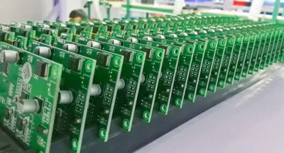
Mass production delivers consistency and cost efficiency at scale. But some applications require custom boards for specific requirements — scientific instruments, advanced research equipment, or specialized industrial controls.
Comparison: Custom vs. Mass Production
| Factor | Mass Production | Custom / Low-Volume |
| Typical quantity | 1,000 – 100,000+ units | 1 – 500 units |
| Per-unit cost | Low | Moderate to High |
| Lead time (setup) | 2-4 weeks (longer) | 1-2 weeks (faster) |
| Flexibility | Limited (hard tooling) | High (soft tooling, manual options) |
| Component sourcing | Volume pricing, longer procurement | May require premium pricing for small quantities |
| Testing approach | Full ICT fixture + FCT | Flying probe + manual FCT |
| Best for | Consumer products, automotive, telecom | R&D, prototypes, medical, aerospace |
Both approaches have their place. The right choice depends on the application, timeline, and budget. Many manufacturers start with custom assembly for prototyping and validation, then transition to mass production once the design is proven.
Need PCB Manufacturing or Assembly?
Get a free quote within 24 hours. We specialize in prototype-to-production PCB/PCBA for hardware teams worldwide.
PCBAndAssembly: Your Partner for Professional PCB Assembly
At PCBAndAssembly, we combine advanced SMT lines with selective through-hole capability to handle mixed-technology boards of all complexities. Our facilities feature:
- Fully automated SMT lines with SPI + pre/post-reflow AOI
- Selective soldering for hybrid SMT/THT assemblies
- X-ray inspection for BGA and QFN verification
- ICT, flying probe, and functional testing options
- ISO 9001-certified quality management
- Lead-free (RoHS-compliant) assembly with full material traceability
- Quick-turn prototype assembly and volume production
Whether you need 10 prototype boards or 10,000 production units, get in touch for a quote: [Contact PCBAndAssembly]
Frequently Asked Questions
What is the difference between SMT and through-hole assembly?
SMT (Surface Mount Technology) mounts components directly onto the PCB surface, enabling higher density and faster assembly. Through-hole technology inserts component leads through drilled holes and solders them on the opposite side, providing stronger mechanical bonds for high-reliability and high-power applications. Most modern boards use a hybrid of both methods.
Which assembly method is better — SMT or through-hole?
Neither is universally better. SMT is preferred for high-density, high-volume, and high-frequency designs. Through-hole is better for connectors, power components, and applications requiring mechanical robustness. The best approach is often a combination of both on the same board.
How long does PCB assembly typically take?
For SMT assembly, a typical run takes 1-3 business days after component availability. Through-hole assembly adds 1-2 days. Full turnkey assembly (including component procurement) typically takes 2-4 weeks for prototype quantities and 3-6 weeks for production volumes. Quick-turn services can accelerate this to 5-10 business days.
What is the most common defect in PCB assembly?
The most common defect category is solder-related — specifically insufficient solder, solder bridging, or cold solder joints. Approximately 80% of SMT defects originate at the solder paste printing stage, which is why 3D SPI inspection has become standard in quality-focused facilities.
What is selective soldering and when is it used?
Selective soldering is a process where a robotic nozzle solders only specific through-hole joints, avoiding thermal stress on nearby SMT components. It is used on mixed-technology boards where SMT parts are already reflowed and THT components need to be added without damaging the existing joints.
How does AI improve PCB assembly quality?
AI is used in AOI systems to reduce false call rates from ~15-20% to under 3%. AI also optimizes reflow oven profiles, predicts maintenance needs for pick-and-place machines, and detects process drift before it produces defects. These improvements increase yield and reduce manual inspection labor.
Can flexible PCBs be assembled using standard SMT processes?
Yes, but special handling is required. Flex circuits need carrier fixtures to maintain flatness during soldering. Thermal profiles may need adjustment due to the lower mass of polyimide substrates. Adhesive reinforcement may be needed at connector attachment points. Many experienced PCBA manufacturers (including PCBAndAssembly) offer dedicated flex assembly capabilities.
Is SMT better than THT?
Neither is universally better. SMT is usually better for density and automated placement. THT is often better for mechanical retention or large leaded components. Many reliable products use mixed technology.
Conclusion
Modern PCB assembly is a controlled system, not a single machine. SMT provides dense and repeatable placement. THT provides mechanical and electrical options for parts that do not fit a surface-mount process. SPI, AOI, X-ray, ICT, and functional test create different layers of evidence. Connected-factory data and newer inspection technologies can improve visibility, but only when the underlying data, recipes, materials, and acceptance criteria are controlled.
Get Quote Free