Flying Probe Test vs ICT: Costs and How to Choose
Flying probe testing is suitable for prototypes and low-volume production. ICT testing is suitable for high-volume production. Before you lock your layout, confirm your test points meet flying probe requirements. Before you request a quote, ask your assembly partner exactly what their test strategy covers and what it costs. Both are cheap to handle now and expensive to fix later.
Get Your PCB Quote!
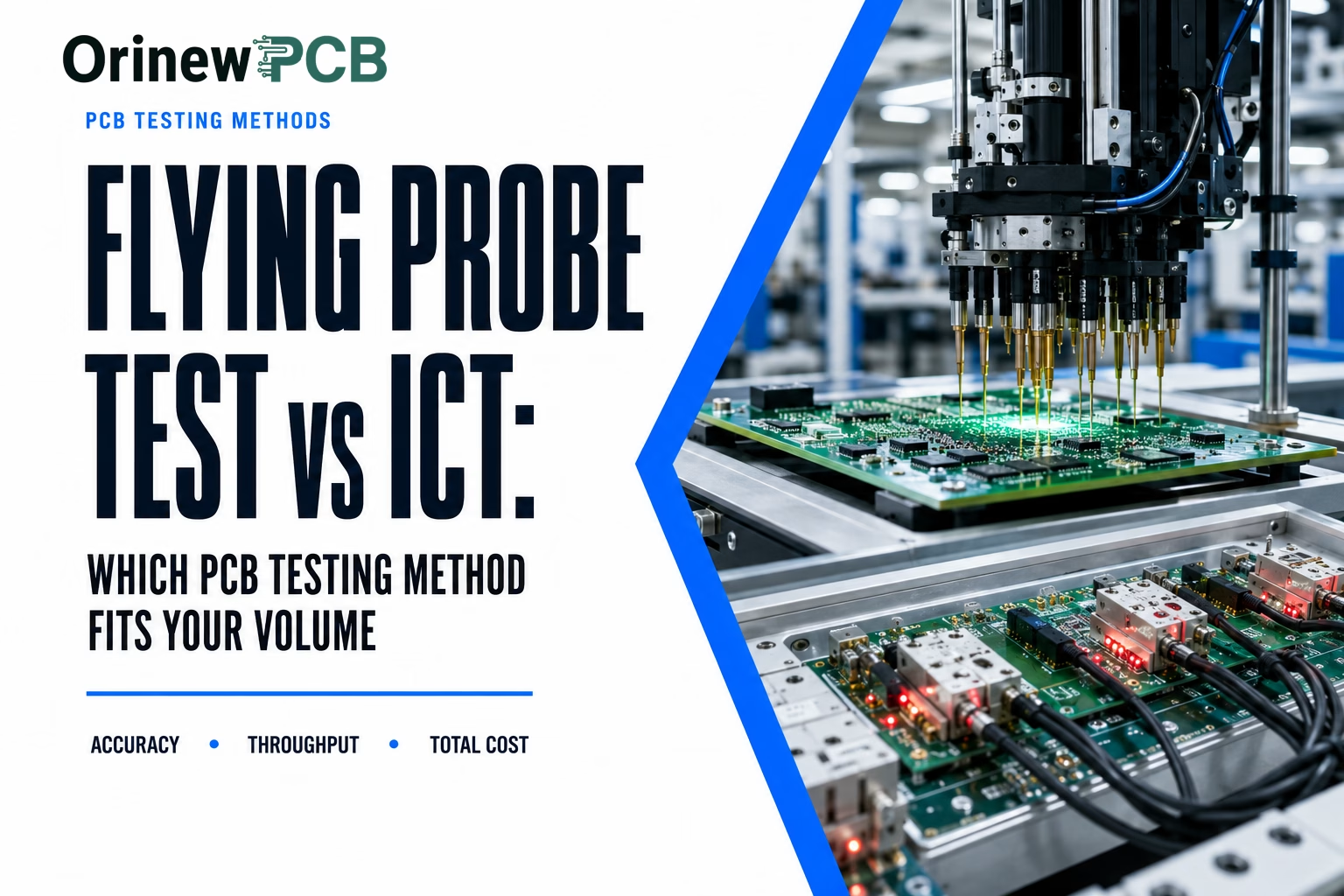
Table of Contents
- Quick Specs
- What is a flying probe test?
- Why ICT gets expensive for small batches
- Flying probe vs ICT: side-by-side comparison
- When to use flying probe vs ICT: the volume breakpoint
- What flying probe testing costs
- How to design test points for flying probe testing
- Where flying probe fits in a full test strategy
- How to ask your assembly partner for the right test
- FAQ
- Conclusion
- References & Sources
Table of Contents
- Quick Specs
- What is a flying probe test?
- Why ICT gets expensive for small batches
- Flying probe vs ICT: side-by-side comparison
- When to use flying probe vs ICT: the volume breakpoint
- What flying probe testing costs
- How to design test points for flying probe testing
- Where flying probe fits in a full test strategy
- How to ask your assembly partner for the right test
- FAQ
- Conclusion
- References & Sources
Flying probe testing is a fixtureless electrical test that checks for opens, shorts, and component value errors, and it is almost always the more cost-effective choice for prototype and low-volume runs below roughly 500 boards. In-circuit testing (ICT) only becomes worth its expensive custom fixture as volume grows into the thousands. This guide explains how both methods work, what each costs, and how to pick the right one for your project—including the test point design rules that determine whether your board can be tested at all.
Quick Specs
| Spec | Value |
| Flying probe test speed | 2-30 minutes per board (complexity dependent) |
| ICT speed | 5-30 seconds per board |
| ICT custom fixture cost | $10,000-$50,000 (vendor-reported) |
| Flying probe fixture cost | None (programming only) |
| Typical breakpoint | Flying probe below ~500 boards; ICT grows attractive in the thousands |
| Flying probe coverage | Opens, shorts, resistance, capacitance, polarity, micro-shorts |
| ICT additional coverage | Powered/logic tests, LED verification, FPGA on-board checks |
Key Takeaways
- Flying probe testing needs no custom fixture, so it is the economical choice for prototypes and low-volume builds; ICT requires a $10,000-$50,000 bed-of-nails fixture.
- As a rule of thumb, flying probe wins below roughly 500 boards; ICT becomes economical only when volume is high enough to amortize the fixture.
- Flying probe checks electrical continuity and component values; it does not replace AOI (solder joints), X-ray (BGA), or functional test (whole-board behavior).
- Test point design must happen at layout time—a board without accessible test points cannot be flying-probe tested at all.
- The real decision is not “flying probe or ICT” but “which test, at which volume, combined with which other methods.”
What is a flying probe test?

A flying probe test (FPT) is an electrical test that uses two to eight programmable probes to contact test points on a board one after another, guided by software generated from the board’s CAD data. With flying probe testing, the probes move and the board stays still—the opposite of a traditional fixture-based test where hundreds of fixed pins contact the board simultaneously.
The test program is generated directly from your design files (typically BOM plus ODB++ or IPC-2581 data), so there is no custom hardware to build. A change to the design means a change to the program, not a new fixture. That is why flying probe fits prototypes, low-volume runs, and boards still being revised.
Flying probe systems verify the electrical integrity of both bare boards and fully assembled boards. On an assembled board, the probes apply low-voltage signals and measure the results to confirm that connections exist, that components are present and correctly valued, and that nothing is shorted.
What a standard flying probe test checks:
- Opens and shorts across nets
- Resistance, capacitance, and inductance values
- Component presence and placement
- Polarity errors
- Micro-shorts and high-resistance defects (advanced systems)
- Phase differences between signal lines (advanced systems)
The cost of that flexibility is speed. Because the probes move from point to point sequentially, a flying probe test takes minutes per board, not seconds. On a board with hundreds of test points, full coverage can take several minutes—one manufacturer’s guide cites roughly 2-30 minutes per board depending on complexity, while others report 5-15 minutes as typical. The spread itself is worth noting: published figures vary with board density, so treat any single number as a starting point, not a promise. Either way, minutes per board is fine for a 50-board prototype run and impractical for a 50,000-board production run.
Why ICT gets expensive for small batches
In-circuit testing (ICT) is the fixture-based alternative. It uses a custom “bed of nails” frame with hundreds of spring-loaded pogo pins, each positioned to contact a specific test point on your board. When the board is pressed down, all pins make contact at once, and the tester runs the full electrical test in seconds.
That speed is ICT’s strength, and it comes from the fixture. The fixture is custom-built for each board design, and it is neither cheap nor fast to produce. Manufacturer-reported fixture costs typically run $10,000-$50,000 depending on board complexity and pin count, and building and debugging a fixture can take days to weeks. If your design changes in a way that moves test points, the fixture may need to be reworked or rebuilt—the role of ICT testing in a production line depends on that fixture staying stable across the run.
For a small run, that fixed cost is fatal. A $20,000 fixture amortized across 100 boards adds $200 per board before you test a single unit. Across 20,000 boards, it adds $1 per board—negligible. That is why ICT is the standard choice for high-volume production and a poor one for prototypes.
ICT is one method in a larger testing picture. It sits alongside AOI, X-ray, and functional test among the three common printed circuit board testing methods used in production.
Flying probe vs ICT: side-by-side comparison
| Criterion | Flying probe (FPT) | In-circuit test (ICT) |
| Best suited for | Prototypes, low-volume, design revisions | High-volume production |
| Fixture requirement | None (software-programmed probes) | Custom bed-of-nails fixture per design |
| Start-up time | Minutes to ~1-2 days (program from CAD) | Days to weeks (fixture design + build + debug) |
| Test speed | 2-30 minutes per board | 5-30 seconds per board |
| Per-board cost (high volume) | Higher ($0.50-$2.00, vendor-reported) | Low (~$0.10, vendor-reported) |
| Up-front cost | Low (programming only) | High ($10,000-$50,000 fixture) |
| Design change flexibility | High (reprogram, often within hours) | Low (fixture rework often required) |
| Coverage | Opens, shorts, RLC values, polarity, micro-shorts | Same as FPT plus powered/logic tests, LED verification, FPGA on-board checks |
| Connector / non-electrical components | Not tested | Not tested |
| Mechanical stress on board | Low (localized probing) | High (simultaneous contact force) |
| Failure diagnostics | Detailed node-by-node isolation | Fast pass/fail with node isolation |
Two rows in that table trip people up more than the rest.
First, ICT is not simply “better coverage.” It adds powered measurements and logic verification that a flying probe cannot do, but it only does so once you have paid for the fixture and only at volumes that justify it. For a low-volume build, the extra coverage is largely theoretical because the fixture cost is unaffordable.
Second, neither method tests everything. Both miss connectors and non-electrical components, and neither verifies that the board works as a whole—that is functional test (FCT). A complete strategy layers several methods rather than betting on one. We cover that combination later in this guide.
When to use flying probe vs ICT: the volume breakpoint
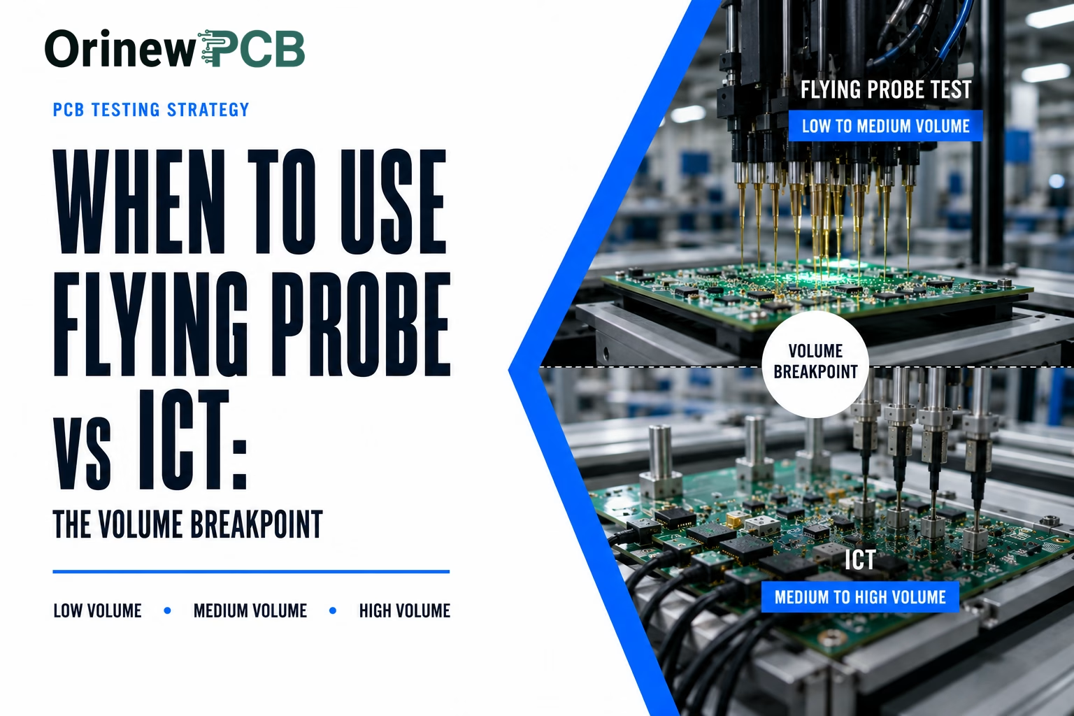
The question that matters most to a buyer: at what volume does ICT stop being a luxury and start paying for itself? There is no fixed answer—it is a calculation—but a practical breakpoint follows from it.
The fixture amortization calculation
An ICT fixture costs money once; flying probe costs more per board forever. The crossover is where the per-board savings of ICT pay for the fixture:
Fixture cost ÷ per-board savings = break-even volume
Plug in realistic vendor-reported numbers: a $20,000 fixture, and ICT saving roughly $1-2 per board in test labor versus flying probe at high volume. That gives a break-even of roughly 10,000-20,000 boards. That gives a break-even of roughly 10,000-20,000 boards. Even at a more optimistic $4-5 per board savings, you need 4,000-5,000 boards to break even.
Practical breakpoint ranges
| Volume | Recommended approach | Reasoning |
| 1-500 boards | Flying probe | Fixture cost is unaffordable; flying probe also tolerates design revisions |
| 500-5,000 boards | Flying probe, or evaluate ICT | Depends on design stability, coverage needs, and fixture quote; run the calculation |
| 5,000+ boards | ICT becomes attractive | Fixture amortizes; per-board test cost drops sharply |
| 50,000+ boards | ICT, often with functional test | Highest test throughput and lowest per-unit cost |
These ranges are directional, not a law. Two factors can shift them.
Design change frequency. If your board is still being revised, every design change can invalidate an ICT fixture. Flying probe absorbs revisions as a software update, often in hours. A project with three expected revisions should stay on flying probe well past the raw volume breakpoint.
Coverage requirements. If your product requires powered logic verification or LED/FPGA checks that only ICT provides, and you have the volume to afford the fixture, ICT earns its cost. If your board is analog and passive-heavy, flying probe covers most of what matters.
We have seen this play out on our own floor more than once: a customer moves to ICT too early, pays for a fixture, revises the design, and pays again. The safer path for an evolving product is flying probe until the design is frozen and volume is proven.
What flying probe testing costs
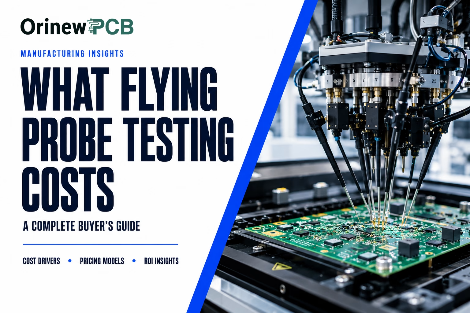
Flying probe testing has a fundamentally different cost shape from ICT: almost no up-front cost, and a per-board cost that scales with test time.
Up-front: There is no fixture. The cost is test program generation from your CAD files and BOM, which is measured in hours of engineering time, not weeks of fixture fabrication—one manufacturer describes having a good flying probe program in around 8 hours.
Per board: The per-board cost is driven by test cycle time. A simple board may test in a couple of minutes; a dense board with hundreds of test points can take 20-30 minutes. At high volume, this per-board cost becomes a real disadvantage—one manufacturer reports per board versus roughly $0.10 for ICT. Both figures are vendor-reported, and they do not agree across sources: different shops quote different ranges depending on board complexity, so treat them as a ballpark rather than a fixed price.
Where flying probe actually saves money: For low-volume runs, the comparison is not per-board cost at all. It is $0 up-front and a few dollars per board versus $10,000-$50,000 up-front. At 200 boards, flying probe wins decisively no matter how you run the math—and testing is just one line item in the total cost of a low-volume PCB assembly.
A worked example
A 100-component, 4-layer board with one BGA. Flying probe test time is estimated at 8 minutes per board. A prototype run of 100 boards means about 13 hours of test time total.
- Flying probe:~$0 program setup beyond engineering time, plus test time. Total testing cost is dominated by the 13 hours of machine time.
- ICT:a fixture quoted at $18,000, plus per-board test time of seconds. Total testing cost is $18,000 plus a few dollars.
For 100 boards, ICT is 50-100x more expensive. For 50,000 boards, the $18,000 fixture spreads to $0.36 per board and ICT’s speed advantage makes it the obvious choice. The crossover is somewhere in the thousands, which is why the volume breakpoint matters more than any single price.
How to design test points for flying probe testing
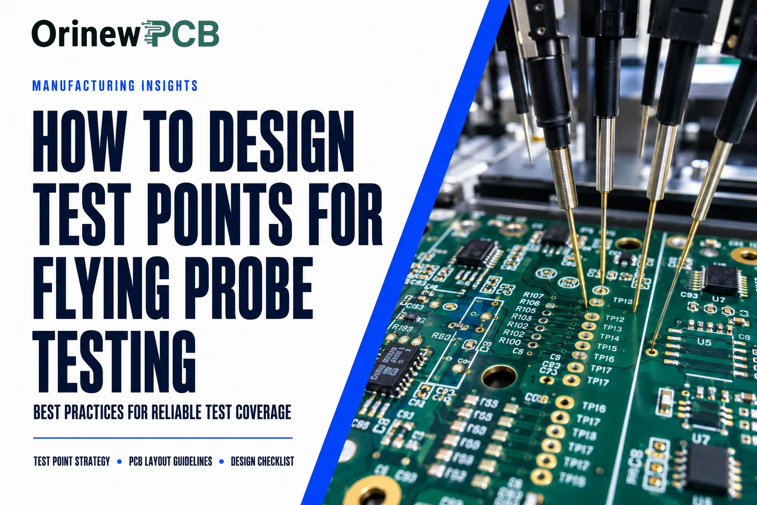
Flying probe testing only works if the probes can reach the nets you need to verify. Test point design is a layout-time decision, and it is the most common reason a board turns out to be untestable. In our DFM reviews, the recurring problem is not exotic—it is boards where test points were squeezed into leftover clearance after the layout was locked, or where critical nets were buried under components with no accessible pad.
Flying probe test point rules:
- Provide accessible test points on all critical nets
- Use test pads at least 6 mil, and prefer 20 mil where space allows for reliable probe contact
- Keep 10-20 mil spacing between test points so probes do not collide
- Keep test points free of solder mask where probe contact is required
- Maintain clearance from tall components and mechanical obstructions
- Include component height data in the CAD files
- Add at least two global fiducials for board alignment
- Use probe-accessible vias (8-20 mil diameter) as test points where pads are not available
- Route traces so they do not obstruct probe access
Design for test, not as an afterthought. The best time to decide which nets require full coverage is at the schematic stage, not after routing. If you wait until the layout is finished, you are negotiating with a locked design—squeezing pads into whatever clearance remains, which is exactly how critical nets end up untestable.
A practical tip: extend small SMD pads or use vias as secondary probe targets when dedicated test pads are tight on space. On dense or high-layer boards, add local fiducials and distribute test points to improve probe reach and cut test time. The goal is not theoretical coverage; it is verified performance where it actually matters.
Where flying probe fits in a full test strategy
No single test method catches everything. A board goes through a layered sequence, and flying probe fills a specific slot in it.
| Layer | Method | What it catches |
| 1 | AOI (Automated Optical Inspection) | Solder joint appearance, component placement, polarity |
| 2 | Flying probe or ICT | Electrical continuity, shorts, component values |
| 3 | X-ray | BGA and hidden solder joints no probe or camera can see |
| 4 | Functional test (FCT) | Whole-board behavior under power |
AOI catches visible solder defects before electrical testing; flying probe or ICT catches electrical faults; X-ray sees inside BGA joints; functional test proves the board does what it is supposed to do. For bare boards, IPC-9252B is the standard that covers electrical test requirements for unpopulated boards, and both flying probe and bed-of-nails methods fall under it—which is why a bare-board continuity check and an assembled-board test are two different processes, not two names for the same thing. The choice of 2D vs 3D AOI technology changes how early a solder defect gets caught, and advanced X-ray inspection is what sees the hidden joints on complex multi-layer assemblies.
A real-world example: a rigid-flex assembly. Consider a medical wearable built on an 8-layer rigid-flex stack with BGAs on both sides, RF shielding, and flex tails that fold into the enclosure. Once the board folds and closes, half the probe access disappears. The working strategy is staged testing:
- Flying probe the rigid sections before the flex is permanently folded.
- Test bare flex before attachment to confirm continuity through all bends and tails.
- X-ray the BGA joints where no pad access exists.
- Functional test post-assembly through debug headers and designed-in connectors.
No single method covers this board. The combination does. The same principle applies to RF boards, where you would not put a pogo pin on a sensitive microstrip—flying probe handles continuity and isolation on power and low-speed digital nets, while RF trace performance is verified with a vector network analyzer after assembly.
The lesson for buyers: when you ask a manufacturer about testing, the right question is not “do you use flying probe?” It is “what is your complete test strategy for my board type?”
How to ask your assembly partner for the right test
Once you know which test you need, the next step is making sure your manufacturer delivers it. These are the questions worth asking before you commit:
- Do you offer flying probe testing, and what is your typical test time per board for my design?
- What test point requirements do you have for my layout? Will my current design be testable as-is?
- What is your test coverage for a board like mine, and what faults will your strategy miss?
- How do you price flying probe versus ICT, and what is your fixture quote for ICT?
- If I revise the design, how does the test program change—and does it cost extra?
- Which other methods (AOI, X-ray, functional test) are included in your standard assembly process?
These questions separate a manufacturer that treats testing as a checkbox from one that treats it as part of the engineering. A partner that answers with specific test times, coverage statements, and honest limitations is one you can plan around. A partner that answers with vague assurances is a risk you can avoid by asking.
At OrinewPCB, testing is part of every assembly rather than an add-on: AOI on every board, flying probe and functional test available, and X-ray for BGA and complex assemblies. When you send us your Gerber files and BOM, our DFM review checks testability before production and flags any test point issues while the design can still be changed.
Need PCB Manufacturing or Assembly?
Get a free quote within 24 hours. We specialize in prototype-to-production PCB/PCBA for hardware teams worldwide.
FAQ
What is a PCB flying probe test?
A flying probe test uses programmable probes that move to contact test points on a board and verify electrical continuity, shorts, and component values. It requires no custom fixture, making it the economical choice for prototypes and low-volume production.
What is ICT testing in PCB?
ICT (in-circuit testing) is a fixture-based electrical test that uses a custom bed-of-nails frame to contact hundreds of test points simultaneously. It is fast and adds powered logic verification, but the custom fixture costs $10,000-$50,000, so it only pays off at high volume.
Is flying probe better than ICT?
Neither is universally better. Flying probe is better for prototypes, low-volume runs, and frequently revised designs because it needs no fixture. ICT is better for high-volume production where its fixture cost amortizes and its speed lowers per-board cost.
How much does flying probe testing cost?
Flying probe has no fixture cost; the main cost is test program generation and per-board test time. Per-board cost is vendor-reported at roughly $0.50-$2.00 at high volume, but for low-volume runs it is far cheaper than ICT because there is no $10,000-$50,000 fixture.
What are the seven types of PCB testing methods?
Common PCB testing methods include AOI (automated optical inspection), flying probe test, in-circuit test (ICT), X-ray inspection, functional test (FCT), burn-in test, and boundary scan. They are complementary: AOI checks solder joints, flying probe and ICT check electrical continuity, X-ray checks hidden joints, and functional test verifies whole-board behavior.
Conclusion
The choice between flying probe and ICT comes down to volume, design stability, and coverage needs, not which method is “better.” Flying probe testing wins for prototypes and low-volume builds because it needs no expensive fixture and absorbs design changes as software updates. ICT wins at high volume because its fixture cost amortizes and its per-board test cost drops to pennies.
Use the volume breakpoint as your starting frame: flying probe below roughly 500 boards, evaluate ICT in the low thousands, and plan on ICT for large production runs. Then weigh design change frequency and coverage requirements, and remember that flying probe is one layer in a strategy that also includes AOI, X-ray, and functional test.
References & Sources
- How flying probe testing works for PCB assembly— flying probe process, coverage, and ICT comparison details
- The flying probe test for PCBs— ICT vs flying probe comparison table and test point design rules
- IPC-9252B: Requirements for Electrical Testing of Unpopulated Printed Boards— current revision (2016), covers flying probe and bed-of-nails test methods for bare boards
- Flying probe test costs: what to expect— vendor-reported cost factors and setup figures
- Flying probe testing: modern PCB quality assurance— vendor-reported test time and per-board cost ranges
- ICT vs flying probe test complete comparison— cost, throughput, and fault coverage comparison
- The bed-of-nails advantage: maximizing test coverage with ICT fixtures— vendor-reported ICT fixture cost range
Get Quote Free