Boosting SMT Yield: 2D vs 3D AOI Technology & Best Practices
AOI technology is a step in modern PCB assembly, crucial for ensuring product quality, improving production efficiency, and enabling intelligent manufacturing.
Get Your PCB Quote!
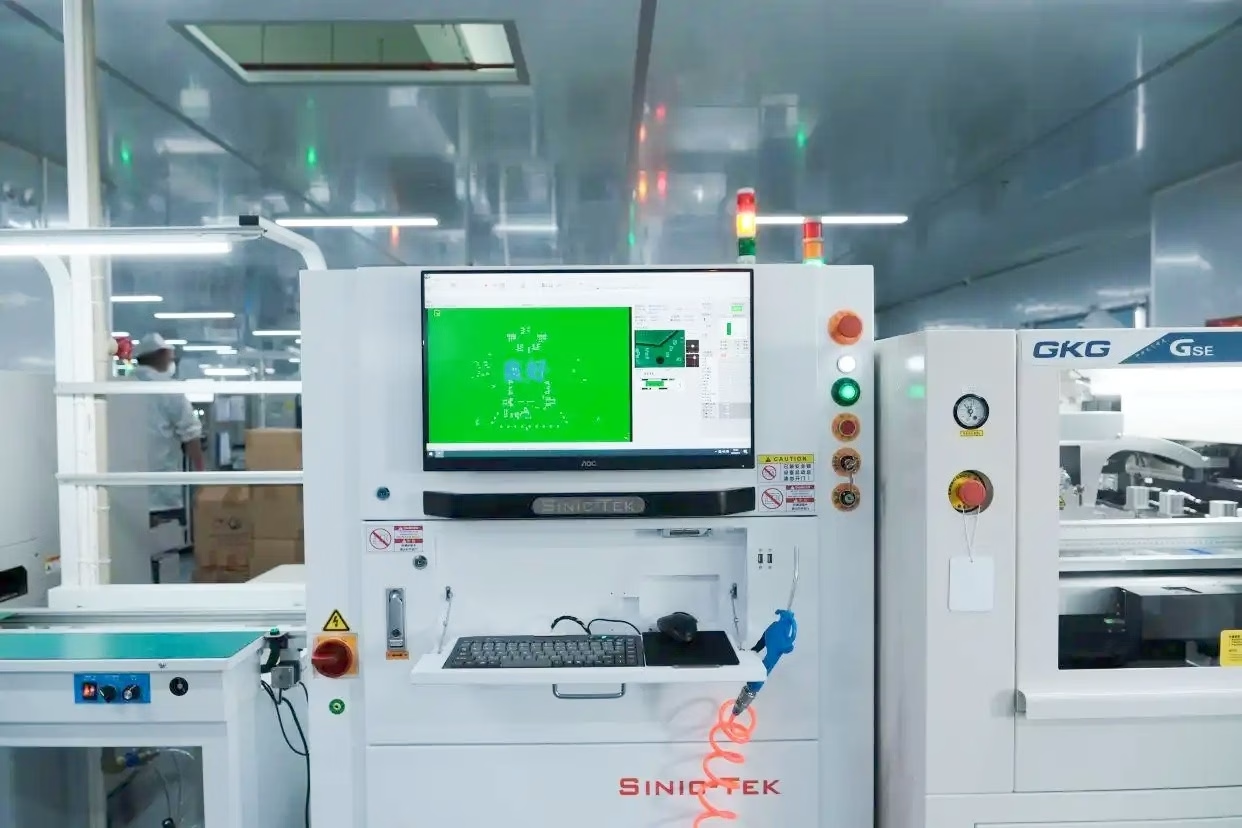
Table of Contents
- 1. What is AOI?
- 2. Why Choose AOI Technology?
- 3. What are the Types of AOI Systems?
- 4. Comparison of AOI with Other Inspection Methods
- 5. The Importance of AOI in PCB Assembly
- 6. What are the Inspection Precautions for AOI?
- 7. Future Development Trends of AOI Technology
- 8. PCB Assembly AOI Technology FAQs
- 9. Summary
Table of Contents
- 1. What is AOI?
- 2. Why Choose AOI Technology?
- 3. What are the Types of AOI Systems?
- 4. Comparison of AOI with Other Inspection Methods
- 5. The Importance of AOI in PCB Assembly
- 6. What are the Inspection Precautions for AOI?
- 7. Future Development Trends of AOI Technology
- 8. PCB Assembly AOI Technology FAQs
- 9. Summary
In the highly automated PCB assembly process, a motherboard transforms from a bare board into a fully functional PCBA product through multiple precision steps, including solder paste printing, component placement, and reflow soldering. During this process, even the slightest defect—such as missed placement, incorrect components, misalignment, solder bridging, or missing parts—can cause the entire product to fail. How can these defects be swiftly and accurately detected during mass production? This is where the “quality guardian” on the production line comes into play— AOI technology.
1. What is AOI?
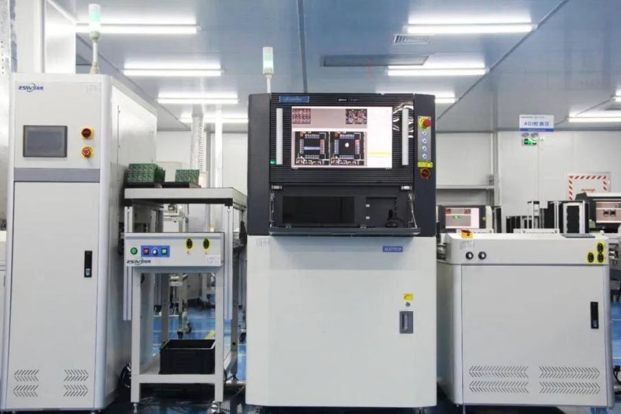
AOI (Automated Optical Inspection) is a critical step in the printed circuit board assembly (PCBA) process. This non-contact inspection method utilizes high-resolution cameras and advanced image processing software to detect and identify defects on PCBA. At PCBAndAssembly, we employ AOI systems to inspect circuit boards at various stages of the assembly process, including post-component placement and post-reflow soldering.
AOI Working Principle:
The core principle of AOI involves comparing captured PCBA solder joint images against preset standards through optical imaging and image processing technology to identify defects. Its workflow consists of four steps:
First, the AOI equipment illuminates the PCBA with RGB light sources from multiple angles, while cameras capture reflected light images. Next, the computer processes the images through noise reduction, enhancement, and other techniques. Then, solder joint quality is determined through color ratio comparison (analyzing red, green, and blue light proportions) or template matching (comparing against standard images). Finally, defects are marked and a report is generated.
Compared to traditional manual inspection, AOI offers the advantages of high speed, reliability, and continuous operation. 3D AOI can add height-related information for visible conditions such as board warpage, package tilt, coplanarity, and lifted leads. It does not directly inspect hidden solder joints beneath package bodies.
2. Why Choose AOI Technology?
AOI technology serves as an indispensable “quality gatekeeper” in PCB assembly. Through high-precision optical imaging and intelligent algorithms, it rapidly and accurately detects minute defects invisible to the human eye—such as solder joint defects, missing or misplaced components, or component misalignment. This significantly enhances inspection efficiency and product yield while reducing labor costs and rework waste.
AOI Core Advantages:
1) High Efficiency & Precision: Inspection speeds are 5-15 times faster than manual methods, identifying defects as small as 0.01mm.
2) Full Process Coverage: Spanning from pre-solder checks to post-soldering final inspections, it ensures quality control throughout the entire production flow.
3) Data-Driven Optimization: Automatically records defect data and generates reports, helping engineers quickly pinpoint process issues and transition from “post-inspection” to “process prevention.”
In short, AOI is a critical tool for ensuring PCB assembly quality, boosting production efficiency, and reducing costs.
3. What are the Types of AOI Systems?
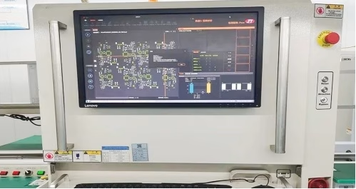
AOI inspection machines in PCB assembly are primarily categorized as follows:
1) By production line position:
Post-Print SPI: Installed after the screen printer and before component placement. SPI measures solder-paste presence, offset, area, height, and volume according to the configured inspection program. It is a separate inspection stage from AOI.
Pre-Reflow AOI: Installed after the placement machine and before the reflow oven. Primarily detects defects after component placement, including missing components, misalignment, tombstoning, incorrect part types, physical damage, and polarity errors.
Post-Reflow AOI: This is the most widely used AOI type. It is capable of simultaneously detecting multiple defects arising from the placement and soldering processes. These defects include solder joint shorts, cold solder joints, insufficient solder bridging.
2) By Camera Structure:
Vertical Camera AOI: Camera lens positioned perpendicular to the PCBA board surface.
Tilted Camera AOI: The camera lens is angled to facilitate inspection of component sides and solder joints.
3) By Light Source Type:
Color Lens AOI: Utilizes red, green, and blue light sources with computer-processed color ratios.
Black-and-White Lens AOI: Uses monochromatic light sources with computer-processed grayscale ratios.
4) By Equipment Operation Mode:
In-line AOI: Equipment directly integrated with the production line. PCBA flows continuously through the line, automatically diverted or advanced after inspection. This method offers high efficiency, suits mass production, and enables fully automated end-to-end inspection.
Off-line AOI: Equipment operates independently. Manual loading of PCBA for inspection is required, followed by manual unloading after inspection. This method offers high flexibility, facilitating focused inspection of specific board types or repaired boards, but efficiency is relatively lower.
5) Classification by Inspection Principle:
2D AOI: Primarily identifies defects through two-dimensional image comparison. This is the most widely used technology, effectively detecting the most common placement and soldering defects.
3D AOI: Uses optical measurement to add height or contour information to visible features. It can improve inspection of coplanarity, lifted leads, package tilt, stand-off, and other height-related conditions. It does not inspect solder joints hidden beneath BGA, QFN, LGA, or bottom-terminated packages.
| Inspection approach | What it evaluates well | Important limit |
| 2D AOI | Visible presence, position, polarity marks, lead condition, solder-bridge appearance, and other plan-view features. | It evaluates contrast, shape, and position from images. It does not directly measure solder-joint volume or inspect joints hidden below a package. |
| 3D AOI | Height, coplanarity, lifted leads, component stand-off, and other visible height-related features when the program and hardware support those measurements. | 3D information improves judgment of visible geometry; it does not turn an optical system into an X-ray system for hidden BGA, QFN, LGA, or bottom-terminated joints. |
Choose 3D AOI when a height-related condition is part of the risk: coplanarity, lead lift, package tilt, or a visible solder-shape question that needs depth information. Choose 2D AOI when the critical checks are visible placement and appearance at the required line speed. The choice depends on the package mix and failure mode, not on a blanket claim that one system replaces the other.
Laser AOI: It is capable of detecting height information, but it features complex programming and slower speeds. It is currently the most expensive AOI system, but offers the highest reliability and precision, even detecting voids within solder joints.
4. Comparison of AOI with Other Inspection Methods
PCB assembly inspection commonly combines Automated Optical Inspection (AOI), solder paste inspection (SPI), Automated X-ray Inspection (AXI), In-Circuit Testing (ICT), flying-probe testing, and functional testing. Each method answers a different question. The correct inspection plan follows the product risk and package mix rather than assuming one tool can provide complete coverage.
AOI, SPI, X-ray, and ICT: different evidence at different stages
| Method | Where it fits | What it contributes | What it does not replace |
| SPI | After solder-paste printing | Paste-deposit control before components are placed. | Placement, reflow-result, hidden-joint, or electrical verification. |
| AOI | After placement and/or after reflow | Fast, repeatable screening of visible placement and workmanship conditions. | Hidden-joint inspection or electrical proof. |
| X-ray | At a defined risk gate, often first article, sampling, or targeted review | Non-destructive visibility into joints concealed by package bodies. | Complete electrical or functional verification. |
| ICT | After assembly, where test access and fixture strategy support it | Electrical checks such as opens, shorts, and selected component values or circuit conditions. | Visual workmanship judgment, hidden-joint image analysis, or end-product functional coverage. |
SPI is the post-print inspection: it checks the solder-paste deposit after printing and before placement. ASC International’s 3D SPI description documents this process position. AOI trend data may reveal symptoms of a drifting process, but neither pre-reflow nor post-reflow AOI measures reflow-oven temperature directly; thermal profiling and oven control use their own process-control methods.
AOI vs. Manual Visual Inspection
AOI operates 5–15 times faster than manual inspection, detecting defects on a board in 10–30 seconds compared to 3–5 minutes for manual inspection. In terms of precision, AOI can detect defects as small as 0.01 mm — ten times finer than manual inspection (0.1 mm) — with a significantly lower error rate. AOI is also more consistent, as it follows pre-set algorithms to ensure uniform standards. Human inspectors, on the other hand, are susceptible to mood and fatigue. However, manual inspection retains cost advantages for small batches and simple PCBA.
AOI vs. X-Ray Inspection
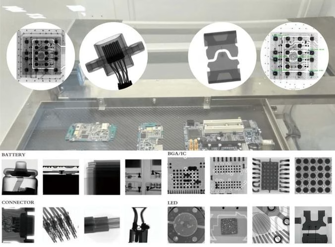
AOI evaluates surface-visible features. It cannot inspect joints hidden beneath packages such as BGAs, LGAs, QFNs, or bottom-terminated components; exposed-lead QFP solder joints remain visible to AOI. X-ray can reveal internal solder-joint conditions in concealed packages, but it does not replace electrical or functional testing.
What AOI can detect, and what it cannot prove
| AOI is well suited to screen | AOI cannot by itself prove |
| Visible missing, wrong, offset, skewed, rotated, tombstoned, or polarity-marked components; exposed-lead and visible solder-bridge conditions; and visible workmanship features defined in the inspection program. | Internal solder-joint structure, hidden BGA-ball conditions, void percentage, internal opens, electrical parametric performance, firmware behavior, or long-term field reliability. |
For hidden solder joints, X-ray is the non-destructive visual method normally considered. Shin-Etsu describes X-ray inspection of BGA soldered areas and voids. The necessary evidence should be defined by the product risk, package types, and acceptance requirements.
AOI vs. Flying Probe Testing
AOI excels at detecting visible workmanship conditions and component misalignment. It may flag visual indications of an open or short, but it cannot confirm electrical continuity. Flying-probe testing focuses on electrical verification and can confirm whether a suspected condition is truly open or conductive. AOI is commonly used for rapid visual screening, while flying-probe testing is useful for prototypes, lower-volume builds, and electrical confirmation where a dedicated ICT fixture is not appropriate.
In a word, AOI technology is merely a tool for fault detection and quality monitoring—not a universal solution for enhancing product quality. One should not expect automatic quality improvement simply by adopting AOI. Only by organically integrating the AOI system into the PCB assembly production and management workflow can the true benefits of this technology be effectively realized.
5. The Importance of AOI in PCB Assembly
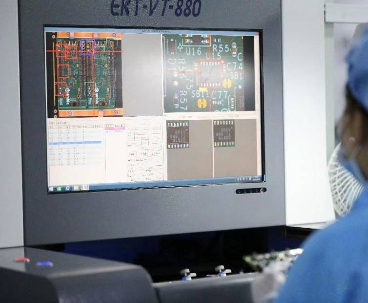
AOI plays a critical role in PCB assembly. By leveraging high-speed imaging and intelligent algorithms, it replaces manual labor for high-precision, high-efficiency defect detection. This core technology ensures product quality, enhances production efficiency, and reduces costs.
1) Enhance inspection efficiency and reduce labor costs
Traditional manual inspection relies on visual observation, which is susceptible to fatigue, experience variations, and other factors, leading to increased missed defect rates and low efficiency. AOI equipment rapidly scans PCBA using high-resolution cameras and compares them against preset standard images. It enables 24/7 continuous operation, achieving inspection speeds far exceeding manual capabilities. This makes it particularly suitable for mass production of high-density, miniaturized PCBA (e.g., mobile phone motherboards, industrial control equipment).
2) Precisely identify defects to reduce rework waste
Through optical imaging and algorithmic analysis, AOI technology detects microscopic defects invisible to the naked eye, including but not limited to:
Soldering Defects: visible bridges, solder balls, exposed-lead wetting or fillet appearance issues, and other visible workmanship conditions defined by the inspection program. Hidden voids require an X-ray or other approved verification method.
Component Issues: misplacement, missing components, polarity errors, tombstoning, sideways placement, etc.
Solder Paste Printing Problems: uneven thickness, positional shifts, printing omissions, etc.
3) Optimize production processes to enhance overall efficiency
AOI equipment serves not only for final inspection but can also be integrated into production lines for real-time monitoring, ensuring quality control at every stage:
Post-Print SPI: Checks solder-paste position, area, height, and volume before placement, so printing drift can be corrected before components are added;
Pre-Reflow AOI: Checks visible component presence, position, orientation, polarity, and placement damage before solder joints form;
Post-Reflow Inspection: Identifies complex defects like missing components or incorrect polarity.
4) Support quality traceability to meet high-reliability demands
During AOI inspection, data for each PCBA board (e.g., images, defect types) is archived to meet quality traceability requirements in high-reliability industries like medical and aerospace. The AOI system automatically records defect types, locations, and frequencies, generating SPC (Statistical Process Control) reports. This helps engineers quickly identify process weaknesses (e.g., insufficient placement machine accuracy, abnormal reflow oven temperature zones) to prevent defects rather than address them after the fact.
6. What are the Inspection Precautions for AOI?
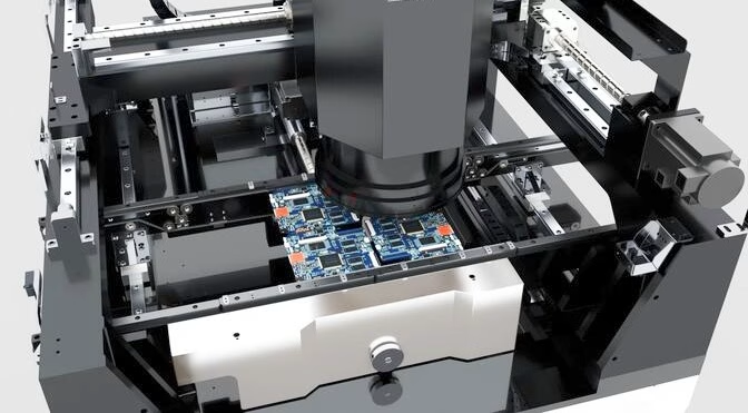
In PCB assembly, AOI inspection is a critical step for quality assurance. Pay special attention to the following points during operation:
1) Pre-Startup Preparation
Ensure the power cord is securely connected and the work surface is clean. Always wear an anti-static wrist strap before operation to prevent static damage to circuit boards. After powering on, wait for the system self-test to complete and verify all indicator lights are functioning normally.
2) Equipment Calibration and Adjustment
Select the appropriate inspection program based on the product type. Enter the calibration interface. Place the standard sample in the inspection area and click the auto-calibration button. The equipment will automatically adjust light intensity and camera focus. After calibration, save the parameters and name the file for future reference.
3) Key Parameter Settings
Set detection sensitivity from the approved workmanship criteria, component package data, and validated known-good and known-bad samples. The inspection region should cover the critical leads, pads, markings, and solder features for the selected component without using a generic buffer value for every package.
4) Inspection Process Operations
Place the PCBA steadily onto the conveyor track, ensuring alignment holes are properly positioned. After initiating the inspection program, closely monitor the real-time imaging display for any stuttering. If the equipment triggers an alarm, immediately pause the process. Use the magnifier function to locate the defect position and manually record the defect type and coordinates.
5) Result Handling and Standards
Passed products should be moved to the green-marked area, while non-conforming (NG) items should be placed in the red isolation box. When exporting inspection reports from the system, name files by batch number and include the inspector’s name and date. If three consecutive defects occur at the same location, immediately notify the production line technician to adjust the pick-and-place machine parameters.
6) Shutdown and Maintenance
After closing the inspection program, wait until the fan has completely stopped before disconnecting the main power supply. Use a lint-free cloth dipped in a dedicated cleaning agent to wipe the camera lens and light source module. Clean debris from the track gaps using cotton swabs. Calibrate equipment accuracy weekly using a calibration plate. Contact the manufacturer for maintenance if the error exceeds 0.02mm.
7) Safety Precautions
Never open protective covers or insert hands into the inspection area while the equipment is operating. If smoke or unusual noises are detected, immediately press the emergency stop button and disconnect the main power switch. When cleaning with alcohol, operate at least 3 meters away from the equipment to prevent liquid splashing onto circuit boards.
8) Common Issues and Solutions
If character detection yields excessive false positives, review the component library, approved marking variations, lighting, board revision, and inspection region before changing the threshold. When blind spots occur, review component spacing, keep-outs, camera access, lighting angle, and the selected inspection method; a layout change alone may not solve an optical limitation.
False-positive handling and SMT process feedback
An AOI alarm is a disposition request, not automatically a defect. Widening every threshold can reduce false calls while allowing genuine defects to escape. An overly sensitive program can also overload operators and delay containment of real defects.
- Verify the board revision, approved BOM/package data, inspection program, and lighting setup before changing a threshold.
- Classify reviewed alarms as confirmed defects, program false calls, or items requiring engineering review, and retain the image and location with the disposition.
- Contain the relevant lot when a true defect repeats or clusters at one reference designator, feeder, stencil aperture, placement position, or reflow-related pattern.
- Correct the upstream cause first: printer setup, stencil condition, component library, feeder, placement program, reflow profile, or incoming material condition.
- Change AOI thresholds through controlled review, then verify the revised program against known-good and known-bad samples before releasing it to production.
This feedback loop turns images and alarm counts into process evidence instead of treating AOI as only a final sorting machine. IPC J-STD-001J addresses materials, methods, and acceptance criteria for soldered electronic assemblies, while IPC-A-610J is the companion acceptability document. IPC explains how the two documents work together.
7. Future Development Trends of AOI Technology
AOI is evolving toward greater intelligence and efficiency, such as through AI-driven smart inspection, predictive maintenance, and flexible inspection technologies to further optimize production processes. For electronics manufacturers, selecting AOI applications suited to their production models—such as pre-solder inspection for high-volume production and post-solder inspection for low-volume, high-mix production—is crucial.
8. PCB Assembly AOI Technology FAQs
Automated optical inspection (AOI) is a machine-based technique used to test and check PCBAs for potential errors, such as surface defects, dimensional defects, and component placement defects.
AOI is based on automated image processing, supported by optical sensors and machine evaluation algorithms. The goal is to automate quality assurance, accelerate processes, and detect errors with the highest accuracy.
AOI is exceptionally useful in maintaining quality standards, especially in high-speed manufacturing lines where manual inspection is impractical.
The core of an AOI system is to acquire high-definition images of the object under inspection using an optical system, and then use image processing algorithms to compare these images with a standard template to identify defects.
9. Summary
AOI technology serves as the “quality guardian” for PCB assembly. Through high-speed, high-precision optical scanning and intelligent algorithms, it detects minute defects such as component misalignment and solder bridging 24/7. This enhances efficiency while reducing missed defect rates, enabling a leap from manual sampling to fully automated process prevention. It safeguards the manufacturing of smart electronic products. With continuous technological advancements, AOI will propel the PCB assembly industry toward higher quality and greater efficiency.
Get Quote Free