
Prototype PCB Manufacturing Services
Validate your PCB design before volume production with custom bare-board prototypes manufactured to your approved Gerber files and specifications.
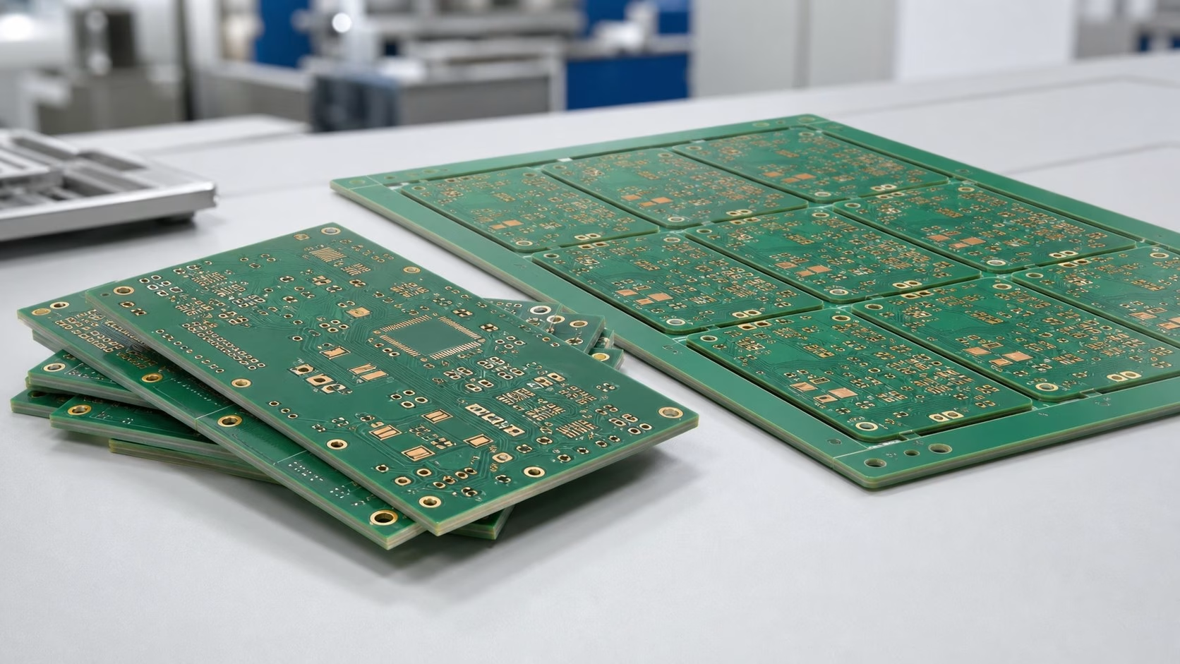
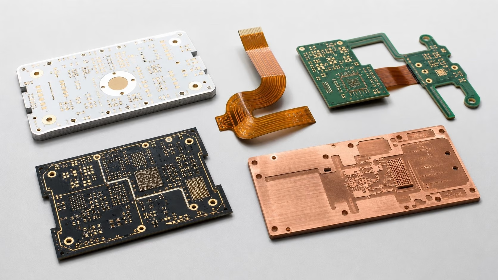
OrinewPCB supports rigid, multilayer, high-frequency, HDI, flexible, and rigid-flex PCB prototypes for engineering validation, functional testing, and pre-production builds. Eligible designs can be produced in as little as 2–7 days after file review and manufacturing approval.
Prototype PCB Manufacturing Capabilities
Choose prototype specifications based on the final product requirements rather than simplifying the board only for testing. Our engineering team reviews the submitted files before production and confirms manufacturability issues, specification conflicts, and missing information.
| Specification | Current published range |
| Board types | Rigid, multilayer, HDI, flexible, and rigid-flex |
| Layer count | 1–8 layers Verify |
| Prototype quantity | 5–100 pieces Verify |
| Build time | 2–7 days for eligible designs Verify |
| Board thickness | 0.4–2.0 mm Verify |
| Board dimensions | 6 × 6 mm to 500 × 500 mm Verify |
| Copper weight | Outer 1–2 oz; inner 0.5–1 oz Verify |
| Minimum trace / spacing | 5 / 6 mil for 1 oz copper Verify |
| Surface finishes | Lead-free HASL, HASL, and ENIG |
| Electrical testing | Flying probe or dedicated test fixture |
Prototype PCB Options for Different Design Requirements
The correct prototype should reproduce the material, stackup, geometry, and electrical requirements that matter in the final product. Select the route that matches the design risk you need to validate.
From files to tested boards
How Our Prototype PCB Manufacturing Process Works
The prototype process is built around controlled revisions. Production begins only after the required files, specifications, and engineering questions have been resolved.
File and Requirement Review
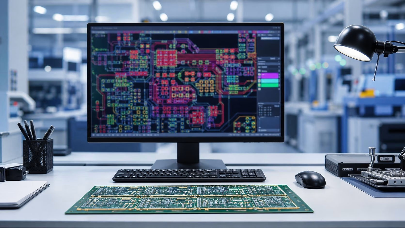
We check the Gerber package, NC drill data, board outline, stackup, material, copper weight, finish, quantity, and delivery requirement for completeness.

DFM and Specification Confirmation
Potential spacing, drill, annular ring, impedance, panelization, and material conflicts are raised before the manufacturing data is released.
Prototype PCB Fabrication
The approved build follows the confirmed stackup and fabrication notes through imaging, etching, lamination, drilling, plating, solder mask, finish, and routing.

Inspection and Electrical Testing
Visual or automated inspection and the agreed electrical test method are used to check the finished boards against the released production data.

Final Review, Packing, and Shipment
Completed boards are checked against the order requirements, protected for transport, and shipped with the agreed documentation.
Evidence before scale-up
Prototype Quality Checks Before Volume Production
A prototype is useful only when it represents the released design and can be traced to the confirmed manufacturing requirements. The test plan should match the risk being validated.
Manufacturing Data Review
Checks whether the files, stackup, drill data, board outline, and fabrication notes describe one consistent revision.
Physical and Visual Inspection
Reviews dimensions, holes, routing, surface condition, solder mask, legend, and other agreed workmanship requirements.
Electrical Test
Uses flying probe or an agreed fixture to check continuity and isolation before the prototype boards are released.
Prototype Only for Appearance
- May use simplified materials or stackup
- May not expose signal-integrity or thermal risks
- Creates another engineering change before production
Prototype for Production Validation
- Uses the intended material and critical specifications
- Supports functional, mechanical, and electrical evaluation
- Creates a clearer path to a controlled volume build
