PCB Assembly Process: From Solder Paste to Final Testing
Follow the PCB assembly process from production-data review and solder paste printing through placement, reflow, inspection, THT assembly, and final testing.
Get Your PCB Quote!
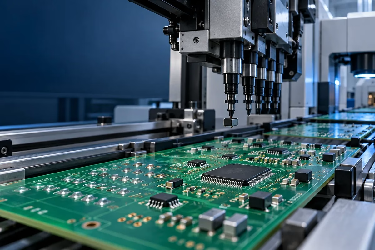
Table of Contents
- Takeaways rápidos
- PCB Assembly Process at a Glance
- What Must Be Ready Before Assembly Starts?
- Step 1: Review Production Data and Set Up the Line
- Etapa 2: Imprimir pasta de solda
- Step 3: Inspect the Solder Paste
- Step 4: Place Surface-Mount Components
- Step 5: Reflow the SMT Solder Joints
- Step 6: Use AOI and X-Ray Where They Fit
- Step 7: Insert and Solder Through-Hole Components When Required
- Step 8: Complete the Specified Cleaning, Test, Coating, and Final Inspection
- PCB Assembly Inspection Methods Compared
- What Changes From Prototype to Production?
- Files to Send for a PCBA Build
- Common PCB Assembly Problems and Their Process Causes
- Perguntas frequentes
- Prepare a PCBA Build for Review
- Sobre este guia
- Referências e fontes
- Related PCB Assembly Guides
Table of Contents
- Takeaways rápidos
- PCB Assembly Process at a Glance
- What Must Be Ready Before Assembly Starts?
- Step 1: Review Production Data and Set Up the Line
- Etapa 2: Imprimir pasta de solda
- Step 3: Inspect the Solder Paste
- Step 4: Place Surface-Mount Components
- Step 5: Reflow the SMT Solder Joints
- Step 6: Use AOI and X-Ray Where They Fit
- Step 7: Insert and Solder Through-Hole Components When Required
- Step 8: Complete the Specified Cleaning, Test, Coating, and Final Inspection
- PCB Assembly Inspection Methods Compared
- What Changes From Prototype to Production?
- Files to Send for a PCBA Build
- Common PCB Assembly Problems and Their Process Causes
- Perguntas frequentes
- Prepare a PCBA Build for Review
- Sobre este guia
- Referências e fontes
- Related PCB Assembly Guides
The PCB assembly process turns a fabricated bare printed circuit board into a working PCBA by mounting components, forming solder joints, inspecting the result, and completing the specified electrical or functional tests. A typical SMT route is solder paste printing, solder paste inspection, pick-and-place, reflow, and optical inspection—but that is only the core route. Through-hole parts, hidden joints, cleaning, coating, and test requirements can add different operations.
This guide explains what happens at each stage, which steps are conditional, and what design files an assembler needs before production starts.
Quick Takeaways
- PCB fabrication and PCB assembly are different processes. Fabrication creates the bare board; assembly attaches and solders components to it.
- There is no single route for every PCBA. Package types, board geometry, volume, reliability requirements, and test strategy determine the actual flow.
- Inspection methods are complementary. SPI checks paste, AOI checks visible features, X-ray examines obscured structures, and electrical tests evaluate circuits or functions.
- Through-hole soldering is a separate routing decision. Wave, selective, and manual soldering are chosen according to the board and production needs.
- Cleaning and conformal coating are not automatic. They should be performed only when the materials, cleanliness criteria, end-use environment, or build specification require them.
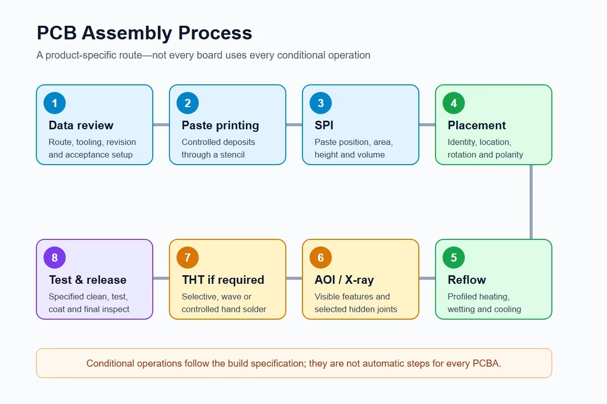
PCB Assembly Process at a Glance
The main SMT path runs from controlled production data to printed paste, placed components, reflowed joints, inspection, and test. The table below shows the job of each stage and why it matters to the build.
| Stage | Main operation | What it controls | Typical output or decision |
|---|---|---|---|
| 1 | Production-data review and line setup | Revision, component orientation, process route, tooling, and acceptance criteria | Released job and line program |
| 2 | Solder paste printing | Paste volume and alignment on SMT pads | Printed panel ready for inspection |
| 3 | Solder paste inspection (SPI) | Deposit position, area, height, and volume | Accept, correct, or stop before placement |
| 4 | Pick-and-place | Component identity, location, rotation, and polarity | Populated but unsoldered board |
| 5 | Reflow soldering | Controlled heating, wetting, and joint formation | Reflowed SMT assembly |
| 6 | AOI and X-ray where appropriate | Visible defects and selected hidden structures | Inspection results and disposition |
| 7 | Through-hole assembly if required | Leaded connectors, large parts, or mechanically loaded components | Completed mixed-technology assembly |
| 8 | Specified cleaning, test, coating, and final inspection | Electrical behavior, workmanship, cleanliness, protection, and release | Accepted PCBA and production records |
This is a routing model, not a universal recipe. A double-sided SMT board may repeat printing, placement, and reflow for the second side. A prototype may use a flexible route, while a stable production build may use dedicated fixtures and more automated controls.
What Must Be Ready Before Assembly Starts?
Assembly should start from one controlled release package. If the BOM says one component revision while the placement file, drawing, or test procedure describes another, the line can faithfully build the wrong product.
At minimum, agree with the assembler on the following inputs:
- fabrication data and the released bare-board revision;
- a BOM with manufacturer part numbers, approved alternatives, quantities, and fitted/not-fitted status;
- centroid or pick-and-place data with reference designators, X/Y coordinates, side, and rotation;
- top and bottom assembly drawings showing polarity, orientation, special placement notes, and variants;
- paste-layer or stencil data plus any special paste or aperture requirements;
- programming files, test procedures, test limits, and connector or fixture requirements where applicable;
- the applicable workmanship standard, revision, acceptance class, and any customer-specific criteria;
- handling requirements for moisture-sensitive, ESD-sensitive, press-fit, heat-sensitive, or otherwise controlled parts.
The exact deliverables vary by assembler and product. Altium’s overview of PCB assembly outputs is a useful starting point, while our guide to PCB fabrication drawings versus assembly drawings explains which decisions belong in each drawing. Before release, use a PCB DFM checklist to catch conflicts that are cheaper to resolve in data than on the line.
Step 1: Review Production Data and Set Up the Line
The first manufacturing step is not soldering. It is translating the released design into a controlled production route.
The assembler checks that the BOM, placement data, Gerber or ODB++ data, drawings, panel information, and revision identifiers agree. The team then prepares the stencil, feeders, nozzles, support tooling, machine programs, inspection programs, and—when required—test fixtures or programming stations.
This review also determines the route. Fine-pitch packages may need tighter printing and inspection controls. Bottom-terminated components can justify X-ray inspection. Heavy or temperature-sensitive parts may be placed after reflow. Through-hole parts may go to selective, wave, or hand soldering rather than through the SMT oven.
Siemens’ discussion of designing for the SMT assembly process shows why footprint, spacing, orientation, and panel decisions affect downstream manufacturability. The important point is simple: line setup follows the actual product, not a generic process diagram.
Step 2: Print Solder Paste
Solder paste printing transfers controlled deposits through stencil apertures onto the SMT pads. Those deposits provide the solder alloy and flux system that will form the joints during reflow.
The printer aligns the stencil with board fiducials, supports the board, and uses a squeegee to fill the apertures. Paste condition, stencil thickness, aperture design, board support, separation settings, and print alignment all affect the deposit. Too little paste can contribute to insufficient joints or opens; excessive or smeared paste can contribute to bridging or solder balls.
Because printing creates the material condition for every downstream SMT joint, a placement machine cannot correct a bad deposit. The fastest machine on the line still needs a stable printing process in front of it.
Step 3: Inspect the Solder Paste
SPI measures the paste before components hide the pads. A 3D SPI system typically evaluates deposit height, area, position, and calculated volume, then compares the result with programmed limits.
The value of SPI is timing: it can expose a printing drift before the board accumulates component value and passes through reflow. It also produces process data that can point to stencil blockage, alignment shifts, support problems, or unstable paste transfer.
SPI does not prove that the final solder joint will be acceptable. It verifies an important upstream condition. Component placement, thermal behavior, pad design, contamination, and other variables can still change the result later.
Step 4: Place Surface-Mount Components
Pick-and-place equipment removes components from reels, trays, tubes, or other feeders, verifies them as the machine is configured to do, and places them into the printed paste at programmed coordinates.
Correct placement depends on more than X and Y position. The production data must also control side, rotation, package, polarity, and reference designator. Feeder setup, nozzle selection, vision recognition, board support, and component presentation then have to match those instructions.
This is why a visually plausible placement file can still be unsafe: an ambiguous rotation convention or incorrect library origin may shift many parts in the same repeatable way. A first-article check should resolve orientation and polarity questions before a larger run continues.
For a closer look at this route, see our SMT assembly overview.
Step 5: Reflow the SMT Solder Joints
Reflow heats the populated board through a controlled thermal profile so the paste activates, the solder alloy melts and wets the intended surfaces, and the joints solidify during cooling.
A commonly described profile includes preheat, a controlled transition or soak region, time above liquidus, peak temperature, and cooling. These names are useful, but they do not define one universal recipe. The correct window depends on the solder paste, board thermal mass, component limitations, surface finishes, joint geometry, and the product specification.
Profiling matters because the oven’s displayed zone temperatures are not the same as the temperatures experienced at every joint. Thermocouples placed on a representative assembly can show whether heavy copper areas, large components, and small components remain within their applicable process limits.
The workmanship requirements should be contractually clear. IPC announced the J revisions of J-STD-001 and IPC-A-610 in 2024, but a purchase order should still state the agreed document, revision, acceptance class, and any exceptions rather than assuming “IPC compliant” is sufficiently precise.
Step 6: Use AOI and X-Ray Where They Fit
After reflow, automated optical inspection compares visible assembly features with programmed criteria. Depending on the equipment and program, AOI can flag missing, shifted, rotated, or polarity-sensitive components and visible solder-joint anomalies.
AOI cannot see through an opaque component body or directly evaluate every internal interface. Ball grid arrays, bottom-terminated packages, and other obscured structures may require X-ray inspection when the design risk and acceptance plan call for it. X-ray works by differences in X-ray attenuation—not infrared imaging—and can reveal information about hidden solder structures that an optical camera cannot see. Nikon describes this use for BGA and electronics inspection in its XT V series overview, and Viscom similarly presents X-ray inspection systems for hidden electronics features.
Neither AOI nor X-ray is a blanket guarantee of product function. Each method needs an inspection plan, appropriate programming, acceptance criteria, and a defined response to flagged results. Learn more about the package-specific route in our BGA assembly guide.
Step 7: Insert and Solder Through-Hole Components When Required
Through-hole assembly is used when the design includes leaded components or connectors that pass through plated holes. In a mixed-technology build, these parts are commonly installed after the main SMT reflow route, although the exact order depends on the product.
The soldering method is conditional:
- Wave soldering exposes selected board areas to a solder wave and suits designs and volumes prepared for that route.
- Selective soldering applies controlled flux, preheat, and solder to programmed through-hole locations while avoiding nearby features.
- Manual soldering provides flexibility for prototypes, rework, low-volume operations, or parts that do not suit automated equipment, but it still requires controlled materials, tools, temperature, technique, and inspection.
One method is not automatically “higher quality” than the others. The correct choice depends on component access, keep-outs, thermal demand, board design, production volume, and acceptance criteria. See our THT PCB assembly overview for the route in more detail.
Step 8: Complete the Specified Cleaning, Test, Coating, and Final Inspection
The final route combines only the operations required by the build. Treating every possible finishing step as mandatory can be as misleading as omitting a required one.
Cleaning
Cleaning depends on the flux system, process residues, cleanliness requirement, component compatibility, downstream coating or bonding needs, and customer specification. “No-clean” is a flux classification, not permission to ignore the actual product environment or coating process. Conversely, cleaning without a validated process can trap contamination or damage sensitive hardware.
Electrical and functional test
Testing should correspond to the design and failure risks. Continuity checks, flying probe, in-circuit test, boundary scan, device programming, and functional test answer different questions. A functional test may show that the product performs defined operations, while an in-circuit method may localize certain assembly faults more efficiently. The test procedure needs explicit limits and a method for recording failures and retest status.
Our PCB assembly testing overview explains how these methods fit together.
Conformal coating and final inspection
Conformal coating is applied only when the product specification and environment justify it. The coating material, masking, thickness, cure, inspection, and keep-out requirements must be defined; coating is not a generic last step for every PCBA.
Final inspection checks the completed assembly against the release package and applicable acceptance criteria. Records may include inspection results, test status, nonconformance disposition, and traceability information required by the customer or quality system.
PCB Assembly Inspection Methods Compared
No single inspection or test method covers paste, visible workmanship, hidden joints, electrical networks, and final product behavior. A defensible plan combines methods according to the package mix and failure risks.
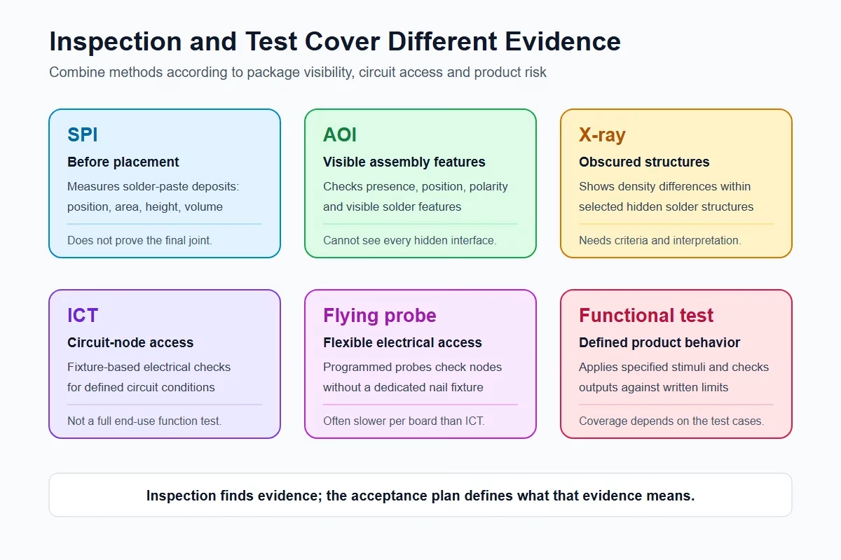
| Method | What it evaluates | Best timing or use | Important limitation |
|---|---|---|---|
| SPI | Solder-paste deposit position, area, height, and volume | Immediately after printing | Does not prove final joint quality |
| AOI | Visible components and solder features | After placement or reflow | Cannot directly see every hidden interface |
| X-ray | Internal or obscured solder structures and density differences | For selected packages, joints, or investigations | Requires suitable equipment, interpretation, and criteria |
| ICT | Electrical access to circuit nodes using a fixture | Stable designs and repeat production where coverage justifies tooling | Fixture/access requirements and not a full end-use function test |
| Flying probe | Programmed electrical probing without a dedicated bed-of-nails fixture | Prototypes and lower-volume builds | Usually slower per board than a dedicated fixture route |
| Functional test | Defined product functions under controlled stimuli and loads | After assembly/programming when product behavior must be checked | Coverage is only as strong as the written test cases and limits |
What Changes From Prototype to Production?
Prototype and production builds use the same physical principles, but they optimize for different constraints. Prototyping emphasizes learning and flexibility; production emphasizes repeatability, controlled changes, throughput, and traceable process performance.
| Decision | Prototype or NPI emphasis | Production emphasis | Buyer consequence |
|---|---|---|---|
| Programming and setup | Fast revision handling and engineering feedback | Locked programs, controlled revisions, verified release | Freeze data before scaling |
| Tooling | Flexible support and low-commitment fixtures where suitable | Durable stencils, fixtures, and repeatable support | Tooling may change after design stabilization |
| Inspection | Broad learning and first-article review | Risk-based coverage with defined limits and reaction plans | Agree which results and records are deliverables |
| Test | Debug access and flexible procedures | Repeatable fixtures, limits, cycle, and traceability | Design-for-test choices affect scale-up |
| Change control | Frequent but documented engineering changes | Formal approval before program, material, or process changes | Never mix revisions in one release package |
A successful prototype is not automatically production-ready. Before scaling, close temporary rework instructions, confirm approved alternatives, validate test coverage, resolve repeated deviations, and release the exact data set that production will use.
Files to Send for a PCBA Build
A quote package can be lighter than a production release, but ambiguity must be visible rather than silently guessed. For production, send a synchronized package with clear revision identifiers.
- Gerber/ODB++ and drill data for the bare PCB, or an agreed equivalent;
- controlled BOM with manufacturer part numbers, approved alternatives, and fitted status;
- centroid/pick-and-place file;
- assembly drawings for both sides and every active variant;
- fabrication drawing, stackup, material, finish, impedance, and other bare-board requirements;
- paste layers or stencil instructions;
- programming files and instructions where required;
- test procedure, limits, interface details, fixtures, and expected records;
- workmanship standard, revision, class, and customer-specific acceptance notes;
- packaging, labeling, traceability, cleanliness, coating, and handling requirements.
Do not rely on filenames such as final_v7_really_final.zip. Put the assembly number, revision, release date, and change authority inside the controlled documentation, and make one person responsible for releasing the package.
Common PCB Assembly Problems and Their Process Causes
A defect label is the start of an investigation, not a complete diagnosis. The same visible symptom can come from design, material, printing, placement, thermal, handling, or test conditions.
| Symptom | Possible process contributors | Prevention or verification path |
|---|---|---|
| Solder bridge | Excess paste, aperture/design interaction, print alignment, placement shift, or wetting behavior | Review paste data and SPI, inspect placement, then evaluate reflow and land design |
| Insufficient solder or open | Low/blocked paste deposit, poor transfer, contamination, coplanarity, or thermal imbalance | Use SPI trends, check stencil/paste handling, inspect leads/pads, and profile representative joints |
| Tombstoned chip component | Unequal wetting forces, pad/thermal imbalance, placement offset, or paste variation | Compare both pads, SPI and placement data; review land and thermal symmetry |
| Shifted or rotated component | Placement data/origin issue, feeder/nozzle/vision problem, poor support, or movement during reflow | Verify first article, library orientation, placement program, support, and paste condition |
| Voids in a hidden joint | Paste volatiles, aperture pattern, surface condition, thermal profile, or joint geometry | Define acceptance criteria first; use X-ray and process experiments appropriate to the package |
| Intermittent electrical failure | Solder defect, damaged part, contamination, connector issue, cracked feature, or incomplete test coverage | Correlate inspection, electrical test, environmental conditions, and failure analysis rather than guessing |
Frequently Asked Questions
What is the difference between a PCB and a PCBA?
A PCB is the fabricated bare board containing conductive features, holes, dielectric layers, solder mask, and markings. A PCBA is that board after the specified components and other hardware have been assembled onto it. PCB fabrication and PCB assembly therefore require different data and production controls.
Is SMT always completed before through-hole assembly?
SMT reflow commonly precedes through-hole insertion in mixed-technology products, but “always” is too strong. The route depends on component temperature limits, access, soldering method, board sides, press-fit operations, cleaning, coating, and other product-specific constraints.
Does every BGA need X-ray inspection?
Not necessarily. BGA joints are hidden, so X-ray is a useful inspection method, but the required coverage should follow the product risk, customer specification, process validation, and acceptance plan. X-ray also does not replace electrical or functional testing.
Does a no-clean flux mean the PCBA must never be cleaned?
No. “No-clean” describes a flux system and its intended residue behavior under defined conditions. Cleaning decisions still depend on the assembly process, contamination, electrical spacing, end-use environment, coating or bonding steps, customer requirements, and a validated cleaning method.
Is conformal coating part of every PCB assembly process?
No. Coating is a specified protective process for products and environments that need it. The material, keep-outs, masking, application, cure, thickness, inspection, and rework rules must be defined; applying an unspecified coating can create new reliability or service problems.
How long does the PCB assembly process take?
There is no responsible universal lead time. Material availability, bare-board readiness, engineering review, tooling, program preparation, quantity, package mix, inspection, test fixtures, programming, coating, and required records all affect the schedule. Compare quotes only after suppliers are pricing the same controlled release and scope.
Prepare a PCBA Build for Review
If you are preparing a prototype or production release, send the board data, BOM, placement file, assembly drawings, quantity, and test requirements. A useful manufacturing review should return specific data questions and a defined assembly route—not just a price with hidden assumptions.
Request a PCB assembly quote →
About This Guide
This article was compiled from published IPC material, electronics-manufacturing guidance, and inspection-equipment documentation. It does not claim unpublished factory test data, a universal process route, or guaranteed defect coverage. It has not been independently reviewed by a licensed engineer; product-specific requirements should be agreed in the controlled build documentation.
References & Sources
- IPC J-STD-001, Requirements for Soldered Electrical and Electronic Assemblies — IPC
- IPC J-STD-001J Table of Contents — IPC
- IPC Releases J Revisions of Two Leading Standards for Electronics Assembly — IPC
- How to Optimize PCB Design for the SMT Assembly Process Flow — Siemens Digital Industries Software
- XT V Series X-ray and CT Inspection — Nikon Industrial Metrology
- X-ray Inspection Systems — Viscom
- PCB Assembly Outputs — Altium Resources
Related PCB Assembly Guides
- SMT Assembly — understand the surface-mount production route.
- THT PCB Assembly — compare through-hole insertion and soldering options.
- Assembly Testing — review inspection and electrical-test choices.
- BGA Assembly — see why hidden-joint packages need a package-specific plan.
Get Quote Free