SMT vs through-hole components: an engineering guide
Compare SMT and through-hole components by mechanical strength, signal integrity, thermal design, assembly cost, and DFM risk before choosing a package.
Get Your PCB Quote!
Table of Contents
- SMT vs through-hole components at a glance
- Mechanical strength: when THT earns its board space
- Electrical performance: parasitics matter before 1 GHz
- Thermal design: choose the heat path, not only the package
- Assembly process: SMT is automated, THT is often selective
- Mixed-technology PCB assembly is often the best answer
- DFM and inspection: make the choice measurable
- Cost and supply chain: compare the finished assembly
- A decision checklist for your next PCB layout
- FAQ
- Conclusion
Table of Contents
- SMT vs through-hole components at a glance
- Mechanical strength: when THT earns its board space
- Electrical performance: parasitics matter before 1 GHz
- Thermal design: choose the heat path, not only the package
- Assembly process: SMT is automated, THT is often selective
- Mixed-technology PCB assembly is often the best answer
- DFM and inspection: make the choice measurable
- Cost and supply chain: compare the finished assembly
- A decision checklist for your next PCB layout
- FAQ
- Conclusion
Choosing between Surface-Mount Technology (SMT) and Through-Hole Technology (THT) is not a contest to find one universally better component style. It is a packaging and manufacturing decision that affects mechanical retention, signal behavior, heat flow, inspection, rework, and the total cost of a finished board.
For most modern electronics, SMT handles the dense, fast, and automated portion of the design. THT remains valuable when a component must tolerate insertion force, vibration, high mechanical load, large thermal mass, or an external heatsink. Many reliable products use both technologies on the same PCB.
The useful question is therefore not “SMT or THT?” It is: which connection style best matches the load, electrical behavior, thermal path, and production process of this component? This guide gives you a practical way to answer that question before layout and sourcing decisions become expensive to change.
SMT vs through-hole components at a glance
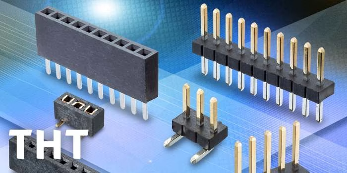
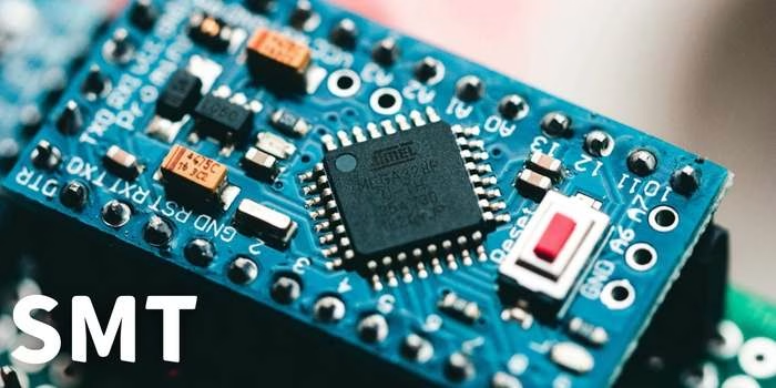
SMT components sit on copper land patterns at the board surface. Their short terminations enable compact placement, short current loops, and automated solder-paste printing, placement, and reflow. THT components use leads that pass through plated-through holes (PTHs), creating a mechanical and electrical connection through the board thickness.
The comparison below is a starting point, not a substitute for the component datasheet or your assembler’s process limits.
| Decision factor | SMT | THT |
| Mechanical load | Good for low-mass parts and loads parallel to the board; vulnerable when a connector or tall component is repeatedly pushed or pulled | Strong through-board anchoring; usually better for connectors, switches, transformers, and parts exposed to shock or vibration |
| Electrical path | Short terminations and small loop area are well suited to fast digital, RF, and low-inductance power paths | Longer leads and plated holes add parasitic inductance and capacitance that must be included in fast nets |
| Thermal design | Heat normally flows into surface copper, exposed pads, and thermal vias | Leads can carry heat into planes, while the package can often connect directly to a chassis heatsink |
| Board density | High density; components can be placed on both sides when clearances and reflow constraints allow | Lower density because each lead needs a drilled hole and routing space |
| Automation | Highly compatible with stencil printing, pick-and-place, and reflow | May require insertion, wave soldering, selective soldering, or manual operations |
| Prototype repair | Fine-pitch and bottom-terminated packages can be difficult to inspect and rework without the right tools | Often easier to hand-solder, probe, replace, and modify during early development |
| Typical best fit | Processors, memory, sensors, passives, fine-pitch logic, compact power stages | High-force connectors, large transformers, power semiconductors with heatsinks, legacy or hand-serviceable parts |
Practical rule: start with SMT when density, short electrical paths, or automated volume assembly dominates. Start with THT when the component itself is part of the product’s mechanical structure. Use a mixed-technology design when the board has both kinds of requirements.
Mechanical strength: when THT earns its board space
The most important mechanical difference is not simply “THT is stronger.” It is how the load travels through the assembly.
An SMT joint is formed between a component termination, solder, and a surface land bonded to the laminate. That structure is effective for small, light components and for loads that do not repeatedly peel or twist the termination away from the board. It becomes a concern when a user mates a connector, presses a switch, pulls a cable, or drops the equipment.
A THT lead passes through the laminate and is soldered inside a plated barrel. The hole and lead provide a through-board load path, so the stress is distributed into the PCB thickness instead of relying only on a surface land. THT is therefore common for USB connectors, terminal blocks, card-edge connectors, relays, large inductors, transformers, and switches with a high actuation force.
Do not use THT as a substitute for mechanical design
THT improves retention, but it does not make an underspecified connector indestructible. Check the connector manufacturer’s mating-cycle, insertion-force, pull-force, and recommended mounting details. For a high-force connector, use a combination of:
- THT signal or power pins where the electrical connection needs through-board support.
- Dedicated THT anchor pins or mounting posts for mechanical load.
- A chassis or enclosure feature that carries cable and mating forces away from the solder joints.
- Keepouts that prevent the connector body from colliding with nearby components during assembly and service.
A common failure pattern in assembly reviews is a connector selected by pin count and pitch alone. The electrical footprint fits, but the board has no mounting support for the cable force. The result is cracked solder, lifted pads, or laminate damage after repeated use. Treat the mechanical drawing as a system requirement, not just a footprint reference.
Electrical performance: parasitics matter before 1 GHz
SMT is usually the safer starting point for high-speed and RF layouts because the connection is short and the current loop is small. That advantage comes from geometry, not from the label “SMT.” A badly routed SMT part can still create a discontinuity, while a carefully constrained THT connection can work at lower speeds.
THT adds lead length and a plated barrel through the stackup. Those structures contribute inductance and capacitance, and the barrel may pass through reference planes or other routing layers. The effect becomes more visible when the signal’s edge rate is fast, even if the clock frequency looks modest. A digital edge with a sub-nanosecond rise time contains significant high-frequency energy; a long lead can behave as a transmission-line discontinuity rather than a harmless wire.
For high-speed nets, review these items before approving a THT package:
- Total lead length from the component termination to the reference plane and destination trace.
- Whether the PTH antipad and clearance interrupt a continuous reference plane.
- The return-current path around the hole field.
- Connector launch geometry, differential-pair symmetry, and via stubs.
- The need for simulation, a controlled-impedance rule, or a prototype measurement.
SMT packages such as QFN, DFN, LGA, and BGA can reduce interconnect length, but they introduce their own risks: hidden solder joints, tighter land-pattern requirements, voiding under thermal pads, and more difficult rework. The right choice is the package that gives the signal a controlled path while remaining inspectable and manufacturable.
Engineering note: do not treat a package’s nominal pitch as a complete signal-integrity specification. The package, escape routing, vias, plane clearances, connector, and stackup form one interconnect. Review that complete path in the same way you would review a cable or transmission line.
Thermal design: choose the heat path, not only the package
Thermal behavior depends on the semiconductor package, copper area, board stackup, airflow, interface material, and enclosure. SMT and THT create different default heat paths.
An SMT power device usually transfers heat through an exposed pad or large soldered termination into the PCB copper. Thermal vias can move heat to internal or bottom copper, but they also introduce design and assembly details. Via size, spacing, solder-mask treatment, paste coverage, copper thickness, and the available plane area all affect the result. Follow the component manufacturer’s recommended land pattern and thermal design rather than copying a generic via array.
A THT power device may conduct heat through substantial leads into the PCB, but many TO-220, TO-247, and similar packages are designed around an external heatsink or chassis interface. That can simplify the board thermal path, while increasing enclosure volume and mechanical assembly work. A THT part is not automatically cooler; it simply gives you a different way to remove heat.
Use this decision path for a power component:
- If the product has a defined chassis heatsink, mechanical attachment, or high-current lead requirement, evaluate THT or a package with a dedicated mounting interface.
- If the product is compact and the board can provide a large copper area and reliable thermal vias, evaluate SMT power packages.
- If the heat load is high enough that the PCB temperature, not the package outline, controls reliability, model the complete thermal path and validate it with a prototype measurement.
- If the component is both hot and mechanically loaded, separate those functions where possible: use a thermal package and a mechanically supported connection instead of asking one solder joint to do everything.
Avoid publishing a single “typical thermal resistance” as though it applies to every layout. Junction-to-ambient performance is strongly layout- and airflow-dependent. Use the supplier’s test conditions and compare them with your actual copper area, via structure, enclosure, and ambient range.
Assembly process: SMT is automated, THT is often selective
The mounting style determines the manufacturing flow, and the manufacturing flow should influence the footprint from the first layout review.
SMT process considerations
SMT normally uses solder-paste printing, inspection of the paste deposit, automated placement, and reflow. The process is repeatable and efficient for large component counts, but it is sensitive to pad geometry, stencil aperture design, component warpage, paste condition, placement accuracy, and thermal profiling.
Important SMT DFM checks include:
- Use the component manufacturer’s recommended land pattern, then verify it against the assembly supplier’s stencil and inspection rules.
- Keep enough courtyard and nozzle access for placement, inspection, and rework.
- Balance copper and thermal mass on two-terminal parts to reduce tombstoning risk.
- Define paste coverage for exposed pads instead of printing one solid aperture that can trap excessive flux volatiles.
- Confirm whether bottom-side components, tall parts, or moisture-sensitive devices affect the reflow sequence.
SMT defects are often process symptoms rather than isolated operator mistakes. Tombstoning can result from unequal pad heating or paste volume. Bridging can result from excessive paste, insufficient solder-mask separation, or placement error. Voiding under a thermal pad can be influenced by aperture design and the reflow profile. A good DFM review connects the defect mechanism to a measurable process control.
THT process considerations
THT may use automated insertion for regular axial, radial, or pin-header parts, but odd-form components often require manual insertion. Soldering can be performed by wave, selective, or hand soldering, depending on the board mix and access.
- Wave soldering is efficient when the board has a compatible component orientation, lead protrusion, and bottom-side keepout.
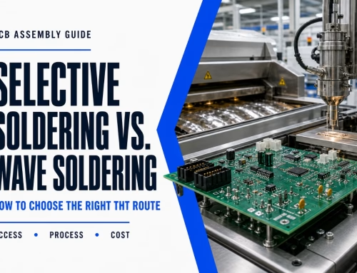
- Selective soldering is useful for mixed-technology boards where a local nozzle can solder THT joints without exposing sensitive SMT parts to a full solder wave.
- Hand soldering is flexible for prototypes and repairs, but it adds labor variation and is difficult to scale without clear work instructions and inspection criteria.
THT design reviews should check hole diameter, annular ring, pad shape, lead protrusion, thermal relief, solder-side access, component orientation, and wave or selective-solder pallets. A footprint that is electrically correct can still be impossible to solder consistently if adjacent copper absorbs heat or the nozzle cannot reach the joint.
Mixed-technology PCB assembly is often the best answer
Most practical boards do not need to choose one technology for every component. A common sequence is SMT placement and reflow first, followed by THT insertion and selective soldering. The exact order depends on component locations, solderability, board orientation, and the assembler’s process capability.
Mixed technology works well when the design assigns each job to the appropriate package:
- SMT for processors, memory, small passives, sensors, and dense power-control circuitry.
- THT for connectors, transformers, large inductors, relays, switches, and parts that receive external force.
- Hybrid packages when signal density requires SMT but the component also needs mechanical anchors.
- Additional brackets, standoffs, or chassis features when the board should not carry the product’s mechanical load.
The trade-off is process complexity. A second assembly stage can require a selective-solder program, a pallet, extra inspection, and additional handling. That cost may be justified by connector reliability, serviceability, or thermal performance. It should be evaluated at the board level, not by comparing the unit price of one SMT resistor with one THT resistor.
DFM and inspection: make the choice measurable
The land pattern and assembly method should be reviewed together. The IPC-7351 land-pattern standard describes generic surface-mount land-pattern principles, including the need to support solder fillets, inspection, testing, and rework. IPC J-STD-001J addresses materials, methods, and acceptance criteria for soldered assemblies, while IPC-A-610J is primarily a visual acceptability standard. These documents complement each other; they are not interchangeable. IPC’s revision announcement explains the different roles of J-STD-001J and IPC-A-610J, and the IPC-A-610J scope and J-STD-001J scope are useful starting points.
For SMT, define how the assembly will verify hidden or fine-pitch joints. AOI can identify many visible placement and solder defects, while X-ray may be needed for BGA, QFN, and other joints that cannot be seen from the surface. For THT, visual inspection may not prove solder fill inside every barrel; the inspection and sampling plan must match the product risk and applicable acceptance class.
Before releasing a design, ask your PCB assembly supplier:
- Which IPC workmanship class and customer acceptance criteria will apply?
- How will hidden SMT joints and selected THT joints be inspected?
- Can the supplier process the smallest pitch, largest thermal pad, and heaviest component in the same build?
- Does the mixed-technology sequence require a pallet, selective-solder tooling, or manual operations?
- What evidence will be included with the shipment: AOI images, X-ray images, test records, or traceability data?
Our practical recommendation is to request a DFM/DFA review using the actual Gerbers, drill files, BOM, pick-and-place data, assembly drawings, and component datasheets. A generic capability statement is less useful than a review of your exact connector, thermal pad, hole pattern, and component clearances.
Cost and supply chain: compare the finished assembly
SMT usually lowers placement labor and supports high component density. THT can increase drilling, insertion, soldering, inspection, and handling cost, especially when many components need manual placement. However, a THT connector may be the lower-cost engineering choice if it prevents a field failure or eliminates a separate mechanical bracket.
For prototypes, THT may be convenient because technicians can insert and hand-solder parts with limited setup. SMT prototypes still benefit from automated placement when the BOM is large, the pitch is fine, or repeated builds are expected. A stencil and feeder setup are not merely costs; they can reduce placement variation and make the next design revision easier to compare.
For production, review these costs together:
- Component price and availability in the required package.
- PCB drilling and routing impact from THT holes and keepouts.
- Stencil, programming, pallet, nozzle, or fixture costs.
- Placement and soldering labor by operation.
- Inspection coverage and expected rework time.
- Changeover time for a mixed-technology process.
- Alternate part availability if the original package becomes constrained.
Do not assume that the smallest component is automatically the best supply-chain choice. A 0201 or fine-pitch leadless part may save board area but reduce second-source options and increase inspection or rework requirements. Conversely, a larger THT part may be easier to source and service but consume routing area and add a separate solder process.
A decision checklist for your next PCB layout
Use the following checklist at schematic capture, footprint approval, and DFM review:
- Mechanical: Will the part receive cable force, button force, shock, vibration, or a heatsink load?
- Electrical: Does the connection sit on a fast edge, RF path, sensitive clock, or high-current loop?
- Thermal: Where must the heat go, and can the board or enclosure provide that path?
- Assembly: Can the selected footprint be printed, placed, soldered, inspected, and reworked with the planned process?
- Density: Is the board area saved by SMT worth the smaller pitch and tighter inspection requirements?
- Service: Will a technician need to replace the part in the field or during validation?
- Supply: Is the package available from more than one approved source, and is the lifecycle acceptable?
- Evidence: What test or inspection record will prove the joint is acceptable?
If the answers conflict, use a mixed-technology solution or add a mechanical feature instead of forcing one package style to solve every problem.
FAQ
Is SMT better than through-hole for every new PCB?
No. SMT is usually the default for compact, automated, and high-density assemblies, but THT is often the better choice for mechanically loaded connectors, large power parts, transformers, and serviceable prototypes. The product’s load case and assembly process should decide.
Can SMT and THT components share one PCB?
Yes. Mixed-technology PCB assembly is common. SMT parts are often reflowed first, followed by THT insertion and selective soldering, wave soldering, or controlled hand soldering. Your board layout must support the complete sequence.
Should a connector always be through-hole?
No. Internal, low-force connectors can work well as SMT parts. A connector exposed to repeated mating, cable pull, or impact usually needs THT anchor pins, a hybrid footprint, or mechanical support from the enclosure.
Is THT better for high-current designs?
Not automatically. Current capacity depends on copper cross-section, temperature rise, contact design, solder joint geometry, and the component rating. THT may provide a useful lead and heatsink interface, while SMT can provide excellent current paths through exposed pads and wide copper. Validate the complete path.
What should I send for an SMT/THT assembly quote?
Send the Gerber or ODB++ files, drill files, BOM, pick-and-place file, assembly drawings, polarity and orientation notes, approved manufacturer part numbers, and the required inspection or functional-test plan. A PCB assembly quote request is more useful when it identifies the mixed-technology sequence and any special THT or thermal requirements.
Conclusion
SMT vs through-hole components is a system decision. Choose SMT when you need compact routing, short electrical paths, automated placement, or dense production. Choose THT when a part must survive mechanical force, connect to an external heatsink, or remain easy to service. Use both when the board combines high-density electronics with mechanically demanding interfaces.
The best time to make that decision is before the footprint is released. Review the mechanical load, electrical path, thermal path, soldering sequence, inspection method, and supply risk together. Then ask your assembler to review the actual design with DFM/DFA feedback. That process catches the expensive mistakes—an unsupported connector, an inaccessible solder joint, an unsuitable thermal pad, or a mixed-technology sequence that cannot be inspected—before they reach production.
For related manufacturing decisions, see the SMT assembly service overview and the PCB assembly testing guide.
Get Quote Free