Automotive PCB: Types, Standards, and Manufacturing Guide
Explore automotive PCB types, standards, materials, manufacturing, and testing. Learn what to specify and verify before requesting a production quote.
Get Your PCB Quote!
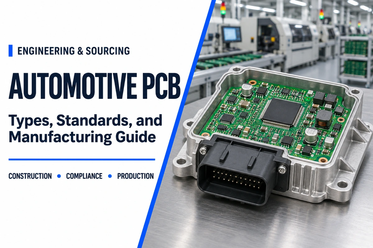
Table of Contents
Table of Contents
An automotive PCB is a high-reliability printed circuit board built to survive extreme thermal swings, continuous road and engine vibration, electrical load-dump transients, and high-voltage isolation demands over a 10- to 15-year vehicle service life. Unlike commercial boards built on standard FR-4, production automotive PCBs pair high-Tg, low-expansion laminates with IPC-6012 Class 3 / IPC-6012FA plating integrity and IATF 16949 / PPAP lot-level traceability.
This engineering and sourcing guide breaks down automotive PCB constructions, maps each industry standard (IATF 16949, IPC-6012FA, AEC-Q100/Q101/Q200, ISO 16750, CISPR 25, ISO 26262, and AIAG PPAP) to its exact deliverable, explains the key material and layout trade-offs, and outlines a complete RFQ verification checklist.
Quick Engineering & Sourcing Takeaways
- Match Laminate to Vehicle Zone: Cabin infotainment modules (-40°C to +85°C) often run reliably on mid-Tg FR-4, whereas under-hood (-40°C to +125°C) and on-engine controllers (-40°C to +150°C) typically require high-Tg, low-CTE laminates (Tg ≥ 170°C, Td ≥ 340°C) to prevent plated through-hole (PTH) barrel fatigue during thermal cycling.
- Enforce Independent Spec Layers: IATF 16949 audits the factory quality system; IPC-6012FA governs bare-board plating (≥ 25 µm average PTH copper for Class 3); J-STD-001JA / IPC-A-610JA control solder workmanship; AEC-Q100/Q101/Q200 qualify individual components; and ISO 16750 / CISPR 25 validate the assembled ECU.
- Cut High-Voltage Creepage via Laminate CTI: On an 800 V DC working-voltage boundary (Pollution Degree 2, Reinforced Isolation per IEC 60664-1), upgrading from standard FR-4 (Material Group IIIa) to a Material Group I (CTI ≥ 600 V) laminate cuts required creepage in half—from 16.0 mm down to 8.0 mm.
- Lock Down RFQ & PPAP Scope Early: Separate recurring unit pricing from NRE, ICT/FCT fixtures, microsection coupon reports, and PPAP Level 3 documentation so competing supplier quotes cover identical verification work.
1. What Is an Automotive PCB?
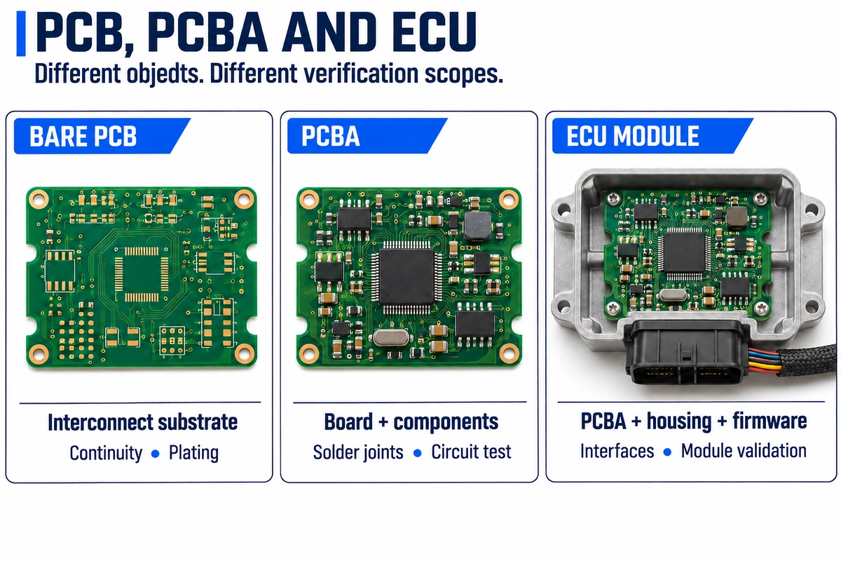
An automotive PCB is the interconnect substrate that mechanically supports and electrically links components across vehicle electronics—from low-voltage body control modules (BCMs) and instrument clusters to 76–81 GHz ADAS radar sensors, battery management systems (BMS), and 400 V / 800 V traction inverters.
In a vehicle, environmental stress—not schematic complexity—dictates board survival. A cabin display controller and a transmission controller may share an 8-layer rigid stack-up, yet the transmission board must endure engine-bay heat, continuous harmonic vibration, and rapid thermal shock from road splash. OEM automotive mission profiles typically target a 10- to 15-year service life (often modeled around 12,000+ active operating hours and tens of thousands of thermal cycles in baseline qualification references such as AEC-Q100 Rev J).
What Is the Difference Between a PCB, PCBA, and Automotive ECU Module?
A PCB is the unpopulated bare substrate; a PCBA adds solder-mounted components; and an ECU module integrates the populated board with firmware, housing seals, thermal interfaces, and harness connectors. Separating these three stages prevents costly testing gaps during PCB manufacturing:
- Bare Printed Circuit Board (PCB): Consists of etched copper layers, prepreg/core dielectrics, plated through-holes (PTHs), microvias, solder mask, and a lead-free surface finish (such as ENIG, Immersion Tin, or OSP). Bare-board verification focuses on 100% netlist continuity and isolation (IPC-9252) alongside cross-sectional plating quality (IPC-6012).
- Printed Circuit Board Assembly (PCBA): Combines the bare board with solder paste, surface-mount passives and fine-pitch ICs (QFNs, BGAs), and press-fit or wave-soldered through-hole connectors. Inspection shifts to 3D solder paste inspection (SPI), automated optical inspection (AOI), 3D X-ray (for BGA voiding and barrel fill), and in-circuit testing (ICT).
- Integrated Automotive Module (ECU / ESA): Protects the PCBA with conformal coating or potting, bonds power devices to heatsinks via thermal interface materials (TIMs), flashes production firmware, and validates the complete electronic subassembly (ESA) against vehicle-level EMC (CISPR 25 / UN ECE R10) and environmental loads (ISO 16750).
2. Automotive PCB Types and Where They Are Used
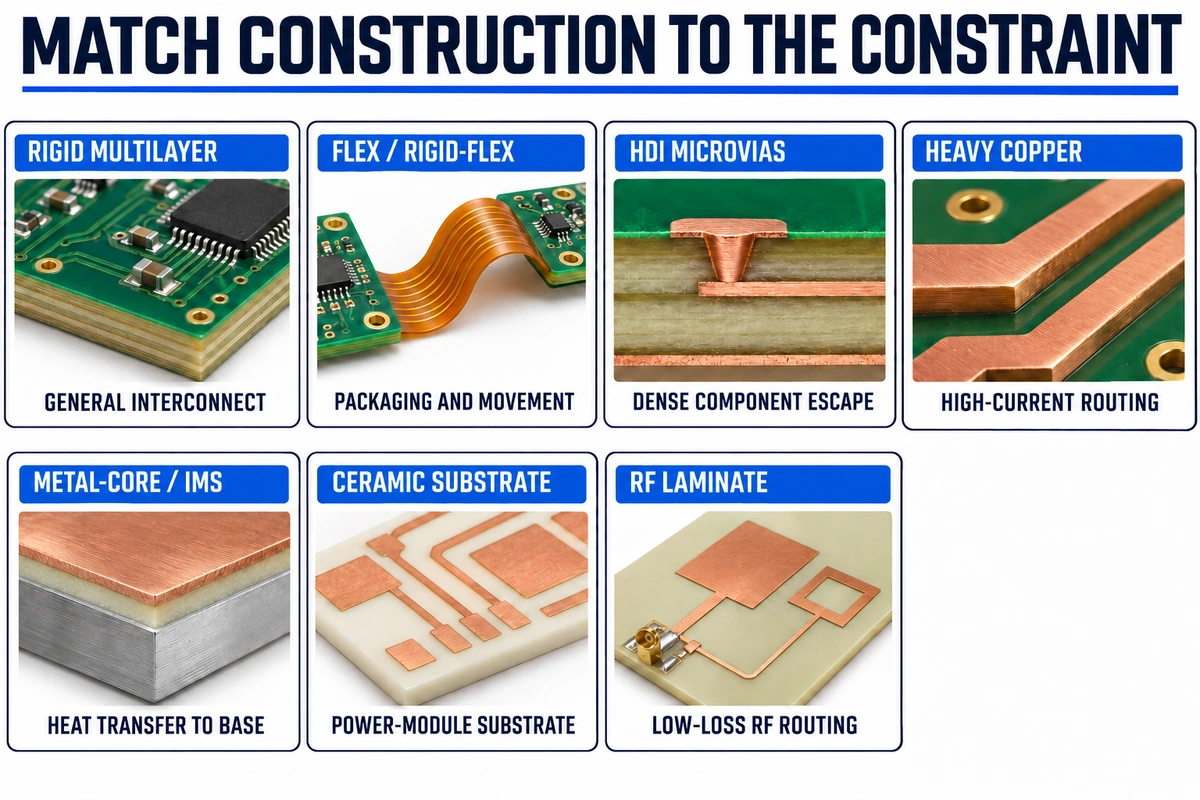
Automotive PCBs span seven core construction and substrate technologies—rigid multilayer, flexible/rigid-flex, HDI microvia, heavy copper, metal-core (IMS), ceramic power substrates, and millimeter-wave RF laminates—which often combine in hybrid stack-ups (such as an HDI digital board bonded to a Rogers RO3003 RF layer for 77 GHz radar).
Use the matrix below to match your dominant physical constraint—routing density, high current, heat flux, packaging envelope, or millimeter-wave loss—to typical substrate benchmarks.
| PCB Construction / Substrate | Target Vehicle Systems | Typical Technical Parameters & Units | Primary Engineering Advantage | Manufacturing & Sourcing Checkpoints |
|---|---|---|---|---|
| Rigid Multilayer (4–16 Layers) | Body control modules (BCM), gateways, digital instrument clusters, low-voltage BMS | Tg 150°C–180°C; Td ≥ 340°C; 1–2 oz (35–70 µm) Cu; PTH Cu ≥ 25 µm (Class 3); dielectric ≥ 75–100 µm | Cost-effective impedance control (50 Ω SE, 100 Ω Ethernet / 120 Ω CAN) and solid ground return planes | Balance copper distribution across the stack-up center to hold bow and twist ≤ 0.75% (IPC-6012 SMT requirement). |
| Flexible & Rigid-Flex (IPC-6013) | Steering-wheel switches, LED headlamp contours, camera interconnects, battery cell-tap harnesses | Polyimide film 12.5–50 µm; RA or ED Cu 18–35 µm; static bend radius ≥ 10× thickness (≥ 20–40× dynamic) | Eliminates bulky wire harnesses and board-to-board connectors that fret under vibration | Specify stiffener thickness (0.2–1.5 mm FR-4/PI/stainless steel), coverlay aperture tolerances, and teardrop transition pads. |
| HDI Microvia (1+N+1 to 3+N+3) | ADAS domain controllers, LiDAR processors, autonomous driving SoCs (0.4–0.65 mm BGA pitch) | Laser microvias 75–125 µm (3–5 mil); aspect ratio ≤ 0.75:1–1:1; line/space 50/50 to 75/75 µm | Escapes high-pin-count FC-BGAs in fewer layers while shortening decoupling loop inductance | Require IPC-WP-023 microvia reliability evidence (IST or 6× reflow + thermal cycling) if using stacked vias. |
| Heavy Copper (3 oz–10 oz+) | Power distribution boxes (PDB), 48 V mild-hybrid DC-DC converters, high-current motor relays | Copper weight 105–350 µm (3–10 oz/ft²); currents 30 A–150 A+; min etch spacing 150–400 µm | Integrates high-current busbars and control logic on one substrate without external cable lugs | Account for lateral etch compensation, resin starvation during lamination (use high-resin prepregs), and reflow thermal mass. |
| Metal-Core / IMS (Al or Cu Base) | Exterior LED headlamps, DRL modules, daytime lighting, directional power stages | Al base 1.0–3.2 mm (5052/6061); dielectric 75–150 µm at 1.0–7.0 W/m·K; HiPot 2.5–4.0 kV AC | Drops thermal resistance from LED/MOSFET junction to heatsink vs. standard FR-4 (~0.3 W/m·K) | Primarily 1- or 2-layer routing; verify dielectric peel strength (≥ 1.0–1.5 N/mm) and HiPot withstand after V-scoring/routing. |
| Ceramic Substrate (Al2O3 / Si3N4 / AlN) | 400 V / 800 V SiC traction inverters, onboard chargers (OBC), high-flux power modules | Al2O3: 24–26 W/m·K; Si3N4: 90–120 W/m·K; AlN: 170–180 W/m·K; DBC/AMB Cu 127–800 µm; CTE 2.5–7.4 ppm/K | Matches Si/SiC die CTE (3–4 ppm/K), provides high insulation strength, and handles > 200°C junctions | Fabricated via Direct Bonded Copper (DBC) or Active Metal Brazing (AMB)—not standard FR-4 etching. Source on a dedicated ceramic line. |
| Millimeter-Wave RF Hybrid (76–81 GHz) | Corner blind-spot radar, forward long-range ACC/AEB radar, V2X antennas | RO3003: Dk 3.00 (10 GHz) / 3.07 (77 GHz), Df 0.0010, TCDk -3 ppm/°C; RO3003G2: Df 0.0011, TCDk -35 ppm/°C | Preserves antenna phase accuracy, gain, and low insertion loss across -40°C to +125°C | Hybrid PTFE/FR-4 lamination requires plasma desmear (CF4/O2), matched press cycles, and zero unauthorized material substitution. |
Rigid and Multilayer PCBs
Standard 4- to 12-layer rigid boards on high-Tg FR-4 serve the majority of vehicle control units, provided the stack-up balances copper symmetrically to keep bow and twist within ≤ 0.75% across lead-free reflow. For CAN FD, Automotive Ethernet, or LVDS camera links, route high-speed layers adjacent to solid reference planes and avoid single-ply prepreg (such as a single 1080 or 106 glass sheet) between power and ground planes—using two plies of prepreg significantly lowers the risk of resin voids and conductive anodic filament (CAF) shorts.
Flexible and Rigid-Flex PCBs
Flexible and rigid-flex PCBs (IPC-6013) replace multi-pin wire harnesses in cramped, vibration-prone areas like steering columns, transmission actuators, and EV battery cell-sense harnesses. Be explicit about whether the flex section is flex-to-install (bent once during assembly, typically requiring a 6× to 10× minimum bend radius) or dynamic flex (bent repeatedly in service, requiring rolled-annealed copper and a 20× to 40× bend radius). Keep plated vias at least 1.25 mm (50 mil) away from the rigid-to-flex transition line, route traces perpendicular to the bend crease, and add strain-relief beads along the interface.
HDI PCBs for Compact ADAS Electronics
High-Density Interconnect (HDI) PCBs use laser-drilled microvias and fine trace/space geometries to break out 0.4 mm–0.65 mm pitch ADAS processors, often reducing layer counts compared to mechanically drilled boards. However, thermal cycling puts heavy axial tensile stress on the interface between the bottom target pad and electroplated microvia copper. As noted in the IPC Standards Revision Table (IPC-WP-023), stacked copper-filled microvias are far more susceptible to target-pad separation during reflow and thermal cycling than staggered microvias. When specifying HDI PCB manufacturing, favor staggered microvias where layout permits, or require lot-level Interconnect Stress Testing (IST) / 6× reflow microsection verification.
Heavy-Copper, Metal-Core, and Ceramic Substrates
High-power automotive electronics rely on three distinct thermal architectures: heavy-copper FR-4 for high-current distribution, insulated metal substrates (IMS) for LED lighting and mid-power switching, and ceramic DBC/AMB substrates for 400 V / 800 V SiC and IGBT traction modules.
As shown in Rogers Corporation’s curamik ceramic substrate datasheet and Rogers’ automotive thermal simulation modeling, picking the right ceramic—Alumina (Al2O3) for cost-sensitive auxiliary stages, Silicon Nitride (Si3N4) for high fracture toughness in 800 V SiC traction inverters, or Aluminum Nitride (AlN) for maximum thermal conductivity—is only half the equation:
- Watch the Thermal Interface Bottleneck: In Rogers’ 200 W SiC die thermal model, pairing a high-conductivity ceramic substrate with a conventional 100 µm Thermal Interface Material (3.4 W/m·K in that model) creates a severe thermal choke point compared to SAC solder (50 W/m·K) or sintered silver (250 W/m·K). Always evaluate the full junction-to-coolant stack when reviewing ceramic PCB options.
High-Frequency PCBs for 76–81 GHz Radar and RF Systems
Automotive millimeter-wave radar (76–77 GHz long-range ACC and 77–81 GHz corner radar) uses ceramic-filled PTFE or hydrocarbon RF laminates laminated into an asymmetrical hybrid stack-up alongside high-Tg FR-4 digital/power layers. At 77 GHz, the wavelength inside a Dk 3.0 substrate is roughly 2.2 mm, meaning minor etching variations, copper roughness, or dielectric thickness shifts can detune patch antennas and degrade angular resolution.
For example, Rogers RO3003 offers Dk = 3.00 (10 GHz), Df = 0.0010, and a thermal coefficient of Dk of -3 ppm/°C, while RO3003G2 lists Df = 0.0011 (10 GHz) and -35 ppm/°C with very low profile (VLP) copper (1.3 dB/inch insertion loss on 5 mil cores). Lock the exact laminate slash sheet and copper foil profile on your master drawing so no substitute material is swapped during procurement.
3. Automotive PCB Standards: What Each One Covers
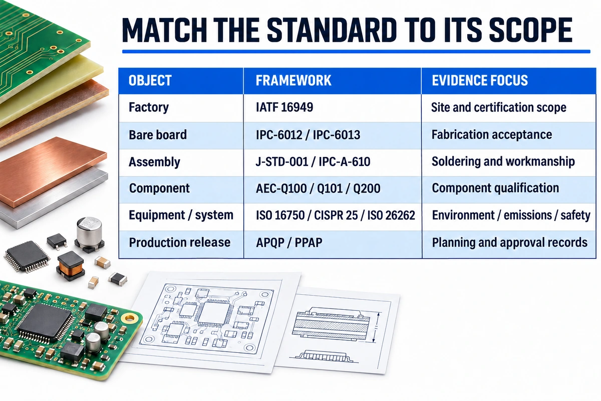
No single “automotive-certified” certificate covers a complete electronic module. Instead, compliance is layered: IATF 16949 audits the factory QMS, IPC-6012FA / IPC-6013 govern bare-board fabrication, J-STD-001JA / IPC-A-610JA control soldering workmanship, AEC-Q100/Q101/Q200 qualify components, ISO 16750 / CISPR 25 / UN R10 validate the assembled ECU, and AIAG APQP / PPAP govern production release.
Use the compliance matrix below to request the exact verification artifact for each risk layer.
| Standard / Framework | Governed Object | Core Quantitative & Process Benchmarks | Mandatory Supplier Deliverable (RFQ / PPAP) | Verification Boundary & Complementary Spec |
|---|---|---|---|---|
| IATF 16949:2016 | Manufacturing facility quality management system (QMS) | Defect prevention, SPC (e.g., Cpk ≥ 1.33 / 1.67 per control plan), PFMEA, internal/supplier audits, lot traceability | Active IATF certificate showing exact physical plant address and scope (“PCB fabrication” vs. “PCBA assembly”) | Certifies factory management processes; pair with IPC-6012FA and PPAP to qualify your specific part number. |
| IPC-6012F + IPC-6012FA | Rigid bare PCB fabrication & automotive addendum | Class 3 PTH Cu ≥ 25 µm avg (20 µm min); 0° breakout; ext ring ≥ 50 µm, int ring ≥ 25 µm; thermal shock microsections | Lot microsection coupon report, bare-board netlist E-test (IPC-9252), impedance TDR report, certificate of conformance (CoC) | Governs rigid bare boards only; use IPC-6013 for flex/rigid-flex and J-STD-001JA for soldering. |
| J-STD-001J + JA / IPC-A-610J + JA | Populated PCBA soldering process & visual workmanship | Class 3 through-hole barrel fill ≥ 75%; minimum end-joint fillet width; BGA void criteria; objective cleanliness validation (SIR/IC) with ROSE for process monitoring | Reflow thermal profile log, SPI/AOI/X-ray inspection data, cleanliness/SIR qualification report | Verifies solder joint geometry and cleanliness; pair with ICT / FCT and ISO 16750 to prove circuit performance. |
| AEC-Q100 / Q101 / Q200 | Integrated circuits (Q100), discrete semiconductors (Q101), passive components (Q200) | Component temperature grades (e.g., Q100 Grades 0–3 from -40°C to +150°C/+85°C); multi-lot zero-fail stress testing (e.g., Q100: 77 pcs × 3 lots, HTOL, TC) | Component manufacturer PPAP & AEC qualification documentation | Qualifies individual packaged components prior to mounting; pair with AEC-Q007 and board-level thermal/vibration validation. |
| ISO 16750-1 to -5 (2023) | Vehicle electrical & electronic equipment (ECU / module level) | Supply transients (Test A up to 101 V / 400 ms on 12 V); vibration 10–2,000 Hz; thermal cycling -40°C to +85°C/+150°C; 85% RH | Design Validation (DV) and Process Validation (PV) environmental & electrical test reports | Explicitly excludes electromagnetic compatibility (EMC); pair with CISPR 25, ISO 11452, and ISO 7637-2. |
| CISPR 25:2021 & UN ECE R10 | Module radiated/conducted emissions & European vehicle/ESA type approval | Broadband/narrowband protection of onboard receivers (150 kHz to 5.9 GHz); immunity to radiated fields and harness transients | Accredited EMC chamber test report; UN ECE R10 E-mark approval certificate (where legally applicable to ESAs) | Applies to populated electronic subassemblies (ESAs) and vehicles—not unpopulated bare PCBs. |
| ISO 26262 (2018) | Safety-related automotive E/E systems (ASIL A through ASIL D) | Hardware architectural metrics (SPFM ≥ 90%–99%, LFM ≥ 60%–90%), random hardware failure target (PMHF < 10 FIT for ASIL D) | Safety Case, FMEDA, DFA (Dependent Failure Analysis), hardware-software interface (HSI), and PCB layout fault-isolation evidence | Allocates functional safety across the system; a bare PCB is never “ASIL certified” in isolation, though layout supports freedom from interference. |
| AIAG APQP (3rd Ed.) & PPAP (4th Ed.) | Product quality planning & serial production part approval (Levels 1–5) | 18 PPAP elements: Design Record, DFMEA/PFMEA, Control Plan, MSA (GR&R < 10%), SPC (Ppk ≥ 1.67), Material Report (IMDS), PSW | Signed Part Submission Warrant (PSW) and commonly PPAP Level 3 full data package prior to SOP | Freezes the approved design, materials, and manufacturing site; any post-PSW change triggers formal PCN and requalification. |
IATF 16949:2016: Auditing the Supplier’s Manufacturing Site
IATF 16949:2016 mandates defect prevention, statistical process control (SPC), PFMEA, and supply-chain traceability. As noted in the IATF official certification overview, certification is site-specific and scope-specific. When qualifying a turnkey supplier, verify whether their certificate covers bare-board fabrication, SMT assembly, or both. If bare boards are subcontracted, require the sub-tier fab’s IATF 16949 certificate and review incoming lot acceptance records.
IPC-6012FA, J-STD-001JA, and IPC-A-610JA: Bare-Board and Assembly Rules
Specify IPC-6012F with the IPC-6012FA Automotive Addendum for rigid bare boards and J-STD-001J / IPC-A-610J (with Automotive Addenda JA) for soldered assemblies, stating Class 2 or Class 3 explicitly on your master drawings.
Per the Global Electronics Association IPC Revision Table, IPC-6012F Table of Contents, and IPC technical papers on HDI registration (E10&S32_03) and copper wrap plating (E8&S06_01), stepping up from Class 2 to Class 3 directly targets thermal-cycling fatigue:
- Thicker Hole-Wall Copper: Class 3 requires ≥ 25 µm average PTH copper (20 µm min) versus ≥ 20 µm average (18 µm min) for Class 2—providing a 25% thicker barrel to resist circumferential cracking during Z-axis expansion.
- Zero Breakout & Tighter Wrap: Class 3 mandates 0° drill breakout (50 µm external / 25 µm internal annular ring) and tighter continuous copper wrap on filled-and-capped vias (documented in IPC technical paper E8&S06_01 as 12 µm for Class 3 vs. 5 µm for Class 2 under IPC-6012 Table 3-2; confirm exact wrap rules against your invoked revision of IPC-6012F/FA).
- IPC-6012FA Enhancements: Tightens criteria beyond base IPC-6012 for lifted lands, dielectric wicking, solder mask thickness, ionic cleanliness, and lot-acceptance thermal-shock microsection coupons.
AEC-Q100, AEC-Q101, and AEC-Q200: Component Stress Qualification
The Automotive Electronics Council (AEC) qualifies ICs (AEC-Q100 Rev J), discrete semiconductors (AEC-Q101), and passives (AEC-Q200) using zero-failure multi-lot accelerated stress testing (such as Q100 Grades 0–3 from -40°C up to +150°C ambient, 77 units × 3 lots per primary test, ELFR screening, and THB/HAST humidity testing per the AEC Document Directory).
Because these standards qualify the packaged component in isolation, the AEC separately publishes AEC-Q007 to evaluate board-level solder joint fatigue after parts are reflowed onto your specific PCB stack-up.
ISO 16750, CISPR 25, UN ECE R10, and ISO 26262
Module-level validation brings together ISO 16750-1:2023 (electrical, mechanical, climatic, and chemical loads), CISPR 25:2021 (RF emissions), UN Regulation No. 10 (European EMC type approval), and ISO 26262-1:2018 (functional safety). Three practical boundaries matter during PCB layout:
- ISO 16750 Excludes EMC: ISO 16750-1:2023 covers power transients, vibration, thermal cycling, and fluid exposure, so always pair it with CISPR 25:2021 and ISO 11452 / ISO 7637-2 for electromagnetic emissions and immunity.
- UN ECE R10 Homologation: For electronic subassemblies (ESAs) sold in UNECE markets, confirm the required amendment series (06 or 07) with your OEM/Tier-1 customer before freezing the EMI filter layout.
- ISO 26262 Is System-Level, Not Bare-Board: An ASIL A–D rating (up to ASIL D with PMHF < 10 FIT and SPFM ≥ 99%) applies to the safety-related system, not a bare PCB in isolation. On the board, functional safety translates into spatial separation between redundant channels, independent power/ground returns, supervisor watchdogs, and CAF-resistant spacing to prevent common-cause hardware faults.
APQP, PPAP, and Customer-Specific Requirements
AIAG APQP (3rd Edition) structures quality planning from concept to launch, while AIAG PPAP (4th Edition) proves—commonly via a PPAP Level 3 submission of 18 elements and a signed Part Submission Warrant (PSW)—that a production run (typically 300 pieces) meets every requirement at rate. Core deliverables include the Design Record, PFMEA, Control Plan, MSA (GR&R < 10%), Initial Process Studies (Ppk / Cpk ≥ 1.67), dimensional/microsection results, IMDS/RoHS/REACH declarations, and Master Sample.
4. Specify Materials and Design Requirements Before Fabrication
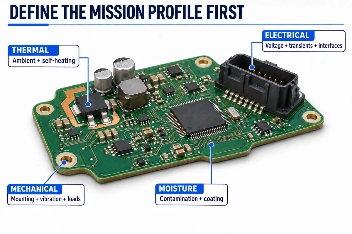
Before releasing Gerber or ODB++ files, translate your module’s vehicle mounting zone and OEM environmental profile into concrete laminate, copper, creepage, and mechanical support rules.
| Vehicle Mounting Zone | Typical Ambient Reference (OEM / AEC-Q100 Grade) | Typical Vibration Profile (ISO 16750-3 Ref) | Typical Laminate & Via Specification | Example Automotive Modules |
|---|---|---|---|---|
| Passenger Cabin (Climate-Controlled) | -40°C to +85°C (Grade 3) | 10–2,000 Hz, lower-level cabin profile (~1.5–3 Grms) | Mid-Tg FR-4 (Tg ≥ 150°C, Td ≥ 325°C, Z-CTE ≤ 3.5%); IPC-6012 Class 2 or Class 3 (20–25 µm PTH Cu) | Infotainment head units, HVAC panels, interior ambient lighting, cabin USB/wireless chargers |
| Cabin Hot Zones / Chassis / Body | -40°C to +105°C (Grade 2) | 10–2,000 Hz, chassis random vibration (~3–6 Grms) | High-Tg FR-4 (IPC-4101/126, Tg ≥ 170°C, Td ≥ 340°C, Z-CTE ≤ 3.0%); IPC-6012 Class 3 (≥ 25 µm PTH Cu) | Body control modules (BCM), seat/door controllers, exterior LED headlamps (IMS), ultrasonic park assist |
| Engine Compartment / Firewall / ADAS | -40°C to +125°C (Grade 1) | 10–2,000 Hz, under-hood profile (~5–12 Grms) | High-Tg filled FR-4 (Tg ≥ 170°C–180°C, Td ≥ 340°C, T288 ≥ 15–30 min, anti-CAF); or RF PTFE (RO3003 for 77 GHz); Class 3 | Engine bay fuse/relay boxes, ABS/ESC brake controllers, 77 GHz forward/corner radar modules |
| On-Engine / Transmission / Mechatronics | -40°C to +150°C (Grade 0) | 10–2,000 Hz, severe engine harmonic (> 10 Grms / 10–30 g) | Ultra-high-Tg FR-4 (Tg ≥ 180°C), polyimide (Tg > 220°C), or ceramic substrate; Class 3 + selective potting/underfill | Transmission control units (TCU), direct fuel-injection ECUs, turbocharger actuators, exhaust NOx sensors |
| EV High-Voltage Battery & Powertrain (400 V / 800 V) | -40°C to +105°C / +125°C (plus I²R self-heating) | 10–2,000 Hz, battery pack/axle shock & vibration (5–15 Grms) | High-Tg FR-4 (often CTI ≥ 600 V Group I) + heavy Cu for BMS/OBC; Si3N4 or AlN AMB/DBC for SiC power stages | Traction inverters, onboard chargers (OBC), HV-LV DC-DC converters, cell-monitoring BMS slave boards |
Note: Exact vibration Grms levels, thermal profiles, and laminate grades must follow your customer’s specific vehicle-zone specification (ISO 16750-3/-4 and OEM CSRs).
Temperature, Thermal Cycling, and Laminate Selection
For lead-free automotive assemblies exposed to under-hood or high-reliability thermal cycling, specify IPC-4101/126 (or /129) filled high-Tg FR-4 (Tg ≥ 170°C, Td ≥ 340°C, T288 ≥ 15 min, Z-axis expansion ≤ 3.0%) and maintain at least a 20°C to 30°C safety margin between peak board temperature (ambient + self-heating) and laminate Tg.
A common mistake is treating Glass Transition Temperature (Tg, measured per IPC-TM-650 Method 2.4.25D) as a maximum operating limit. In reality, Tg is the point where the epoxy matrix softens from rigid to rubbery. Below Tg, an IPC-4101/126 laminate expands along the Z-axis at α1 ≤ 50–60 ppm/°C (already ~3× faster than copper’s 17 ppm/°C). Above Tg, Z-axis expansion jumps 5-fold (α2 ≤ 250–300 ppm/°C), stretching plated through-hole barrels like a mechanical jack during lead-free reflow and thermal shock (IPC E14&S05-05).
Current, Voltage, Creepage, and Clearance (12 V / 48 V vs. 400 V / 800 V EV)
In EVs and hybrids, circuits interfacing across high-voltage boundaries (such as 400 V and 800 V battery packs, OBCs, and traction inverters isolated from 12 V CAN/LIN buses) must be sized according to the actual working voltage across the isolation barrier, pollution degree (PD2 or PD3), and required insulation grade (Basic vs. Reinforced) under IEC 60664-1 and applicable EV safety standards.
Per Texas Instruments’ High-Voltage Creepage and Clearance Design Guide (SLUP419) and Infineon’s IEC 60664-1:2020 Automotive Insulation Coordination Note, laminate Comparative Tracking Index (CTI) dramatically reduces creepage (surface tracking distance), where Reinforced Isolation requires 2× Basic creepage:
- Material Group IIIa (175 V ≤ CTI < 400 V, standard FR-4): Requires 8.0 mm reinforced creepage at 400 V and 16.0 mm at 800 V (Pollution Degree 2).
- Material Group II (400 V ≤ CTI < 600 V): Cuts reinforced creepage to 5.6 mm at 400 V and 11.2 mm at 800 V.
- Material Group I (CTI ≥ 600 V, high-CTI resin/polyimide): Cuts reinforced creepage to 4.0 mm at 400 V and 8.0 mm at 800 V—saving 50% of surface creepage spacing.
For clearance (shortest distance through air), note that the 2× creepage rule does not automatically apply—safety clearances are derived from impulse withstand voltage and overvoltage category, and must include altitude correction multipliers (up to 1.48× at 5,000 m per IEC 60664-1 Table A.2). Similarly, do not confuse functional spacing reductions under IPC-2221B (such as conformal-coated external clearance) with safety insulation barriers; any clearance reduction via conformal coating must satisfy the governing safety standard’s qualification and process-validation requirements (TI SLUP419). Where pin pitch restricts surface creepage, mill a PCB isolation slot at least 1.0 mm wide for Pollution Degree 2 (1.5 mm for PD3).
Signal Integrity, EMC, and ISO 16750-2 Power-Supply Transients
Bench supplies never replicate alternator and starter transients. Per Monolithic Power Systems’ Transient Primer, Texas Instruments’ ISO 16750-2 Load-Dump Overview, and Analog Devices’ Surge Protection Guide, your PCB power-input stage and signal routing must handle three waveforms:
- Load Dump (ISO 16750-2 Test A / Test B, corresponding to legacy ISO 7637-2 Pulse 5a / 5b): When a battery disconnects while the alternator is charging, an unsuppressed alternator (Test A / Pulse 5a) drives 79 V to 101 V on 12 V systems for up to 400 ms; centrally clamped alternators (Test B / Pulse 5b) cap this to 32 V–40 V. Place TVS diodes or active surge-stopper MOSFETs right at the connector pins with wide, low-inductance copper pours so surge currents do not couple into ground planes.
- Cold Cranking & Reverse Polarity: Cold-weather starter engagement pulls a 12 V bus down to 2.8 V–6.0 V, while reversed jump-start cables apply -14 V for up to 60 seconds.
- Controlled Impedance & Return Paths: Specify controlled-impedance tolerances separately by interface—typically 100 Ω ± 10% differential for Automotive Ethernet (100BASE-T1 / 1000BASE-T1), 120 Ω nominal characteristic impedance for high-speed CAN / CAN FD per Analog Devices AN-1123 (confirming exact PCB trace targets against your transceiver and harness design), and 50 Ω ± 5% for RF feeds. Place ground stitching vias within 1.0 mm–2.0 mm of signal layer transitions to keep CISPR 25 radiated emissions in check.
Vibration, Moisture, CAF Resistance, and Mechanical Support
Space mounting standoffs to keep the PCB’s first natural resonant frequency above 200 Hz–300 Hz under 10–2,000 Hz vibration, and coordinate three environmental safeguards:
- Component Staking & Flex-Term MLCCs: Keep ceramic MLCCs (prefer AEC-Q200 soft-termination parts) at least 3.0 mm–5.0 mm away from board edges, depanelization tabs, and screw holes, oriented parallel to the flex axis. Stake tall electrolytic capacitors, inductors, and heavy connectors with neutral-cure RTV silicone or structural epoxy.
- CAF Prevention (IPC-TM-650 2.6.25C): Under DC bias and humidity, copper salts can migrate along glass-epoxy interfaces. Specify anti-CAF laminates (tested 500 hours at 85% RH under 100 V DC bias), stagger high-voltage vias off shared 0°/90° glass-weave axes, and maintain adequate hole-wall-to-hole-wall spacing (≥ 0.4–0.8 mm).
- Conformal Coating (IPC-CC-830): Apply acrylic, polyurethane, or silicone conformal coating (25 µm–75 µm typical dry film) to protect outer layers from condensation and salt spray; see our conformal-coating guide for material selection and masking rules.
5. Automotive PCB Manufacturing: From DFM to Assembly
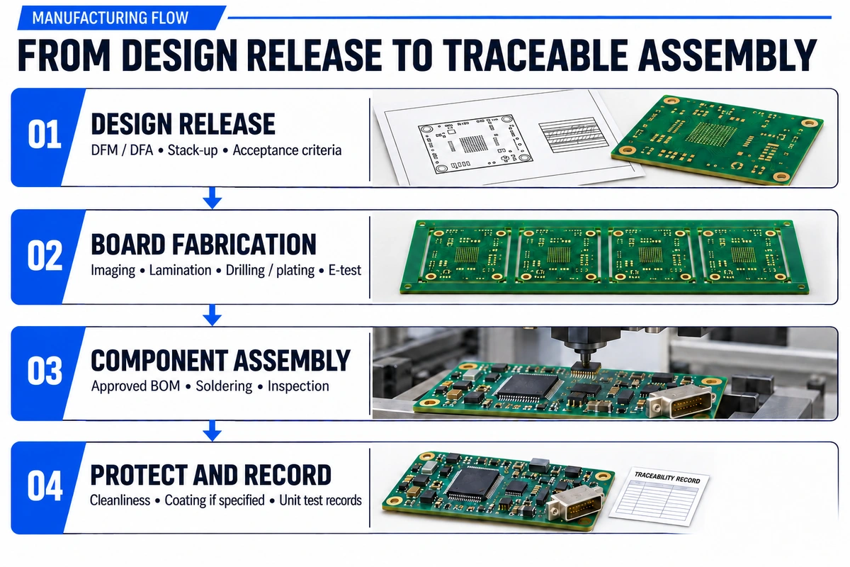
Automotive PCB production enforces closed-loop controls across four sequential phases—DFM/DFA release, bare-board fabrication, SMT/THT assembly, and cleanliness/traceability verification—before volume launch.
Step 1: Review the Released Design (DFM / DFA) and Freeze Acceptance Criteria
Run a formal DFM/DFA audit before cutting tooling using a structured PCB DFM checklist. On the bare board, verify minimum trace/space, CAD annular rings sized to guarantee ≥ 50 µm finished Class 3 external rings after drill wander, drill-to-copper clearances (≥ 200–250 µm) to suppress CAF, and LPI solder mask dams (≥ 75–100 µm) to prevent bridging on fine-pitch ICs. On the assembly side, confirm IPC-7351 footprints, thermal-relief spokes on grounded through-hole pins, global/local fiducials, and accessible ICT test pads.
Step 2: Fabricate the Bare Board (6 Controlled Stages)
- Inner-Layer Imaging, Etching & AOI: Print and etch inner cores, run 100% inner-layer AOI (zero open/short escapes), and apply oxide treatment for lamination adhesion.
- Controlled Lay-Up & Vacuum Lamination: Stack cores with multi-ply B-stage prepreg and outer copper foils, cure under controlled vacuum/temperature/pressure profiles, and verify registration via X-ray targets.
- CNC/Laser Drilling, Desmear & Copper Plating: Drill through-holes (or laser microvias for HDI), remove resin smear via permanganate or plasma desmear, and electroplate ≥ 25 µm average hole-wall copper (IPC-6012 Class 3) with zero plating voids.
- Outer-Layer Imaging, Pattern Plating & Etching: Image outer layers, pattern-plate traces and holes, and etch exposed copper while holding controlled-impedance trace widths within ±10%.
- LPI Solder Mask & Surface Finish: Apply and cure LPI solder mask, then deposit the specified lead-free finish (ENIG, Immersion Tin for press-fit zones, Immersion Silver, or OSP).
- Profiling, 100% Netlist E-Test & Microsection Release: Route or V-score panels, run 100% flying-probe or fixture continuity/isolation testing (IPC-9252), and cross-section coupons after a 288°C (10 s) solder float (IPC-TM-650 2.6.8) to verify plating thickness, resin recession, and annular ring compliance.
Step 3: Source Authentic Components and Assemble the PCBA
Source strictly from the customer’s Approved Vendor List (AVL), log lot/date codes into the Manufacturing Execution System (MES) at incoming inspection, and store moisture-sensitive devices (MSL 2–5a) in dry cabinets per IPC/JEDEC J-STD-033.
During SMT assembly, print SAC305 or high-reliability doped lead-free paste (such as Innolot for +125°C/+150°C under-hood fatigue resistance), verify 100% of pads via 3D SPI, and reflow under nitrogen (N2) using a thermocouple-verified thermal profile. For harness headers, use either compliant press-fit pins (requiring tight ±0.05 mm finished hole tolerances) or nitrogen-inerted selective wave soldering achieving ≥ 75% vertical barrel fill (J-STD-001 Class 3).
Step 4: Control Cleanliness, Conformal Coating, and Unit-Level Traceability
Laser-mark a 2D DataMatrix barcode on every sub-board to tie component lots, reflow profiles, and test logs together. As documented in the IPC J-STD-001H/J release and the IPC Technical Study on SIR and Ionic Cleanliness (E39&S13_02), modern J-STD-001J / JA cleanliness programs no longer accept legacy ROSE limits (< 1.56 µg/cm² NaCl eq.) as standalone process qualification—they require objective evidence via Surface Insulation Resistance (SIR) testing (85°C / 85% RH under bias) or Ion Chromatography to prove flux residues and conformal coatings are electrochemically compatible, reserving ROSE strictly for ongoing production process monitoring.
6. Inspection, Reliability Testing, and Production Approval
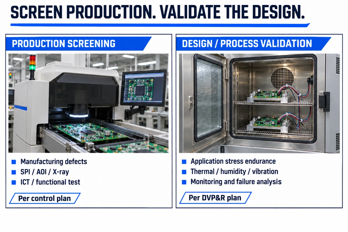
A sound automotive quality plan separates inline non-destructive screening (which catches manufacturing defects during production) from destructive DVP&R qualification (which proves design margin over the vehicle mission profile).
| Verification Method | Typical Stage & Sampling Scope | Target Defects & Typical Test Parameters | Required Quality Record | Coverage Boundary (Next Required Gate) |
|---|---|---|---|---|
| Bare-Board Netlist E-Test (IPC-9252) | Bare PCB final gate (100% of boards via flying probe or universal fixture) | Opens (> 10–50 Ω), shorts/leakage (< 10–100 MΩ at 100–250 V DC), HiPot dielectric breakdown (500–1,500 V DC) | Automated E-test pass log + 2D barcode/ink stamp per array | Confirms netlist connectivity at room temperature; follow with TDR and microsection coupons. |
| TDR Impedance & Microsection Analysis | Bare PCB lot release (1–2 coupons per production panel / lot) | Single-ended (50 Ω) & differential (100 Ω Ethernet / 120 Ω CAN) impedance; PTH copper ≥ 25 µm after 288°C / 10 s solder float | TDR waveform report + metallographic cross-section photos (IPC-TM-650 2.1.1) | Verifies bare-board geometry and plating; follow with 3D SPI / AOI / AXI during assembly. |
| 3D SPI + 3D AOI (IPC-A-610JA) | SMT line inline (commonly 100% post-print and post-reflow) | Solder paste volume/height, bridging, missing/tombstoned/skewed parts, meniscus wetting fillets | Inline SPC defect pareto + archived optical images linked by serial number | Cannot see hidden joints beneath BGA/QFN/LGA bodies; pair with 3D AXI X-ray. |
| 3D Automated X-Ray Inspection (AXI) | Post-reflow / post-selective solder (100% on critical BGAs/QFNs/power pads or per control plan) | BGA head-in-pillow (HiP), solder bridging, thermal-pad voiding (program-specific, often < 15–25%), THT barrel fill (≥ 75% Class 3) | X-ray slice radiographs + automated void-percentage and barrel-fill reports | Confirms physical solder geometry; follow with ICT and FCT to verify electrical operation. |
| In-Circuit Testing (ICT / Flying Probe) | Assembled PCBA (bed-of-nails fixture in volume; flying probe in NPI) | Passive values (R, L, C), diode/transistor orientation, power-rail shorts, powered/unpowered IC pin opens (boundary scan/JTAG) | Per-board ICT pass/fail parametric log tied to unit MES serial number | Tests individual node values at static conditions; follow with Functional Testing (FCT). |
| Functional Testing (FCT / Burn-In) | Final PCBA / ECU gate (custom PXI/CAN/LIN test rig) | Bootloader/firmware flash, ADC/DAC calibration, CAN FD / Ethernet communication, load switching, sleep/quiescent current per spec | Serialized FCT parametric log (e.g., Cpk ≥ 1.67 on key outputs) + firmware checksum | Validates room-temp (or ESS chamber) function; pair with DVP&R / ISO 16750 for lifetime qualification. |
| Environmental & Reliability Validation (DVP&R) | DV / PV qualification & periodic lot requalification | Thermal shock (-40°C to +125°C/+150°C), THB/CAF (85°C/85% RH), ISO 16750-3 vibration (10–2,000 Hz) per DVP&R plan | Accredited lab DV/PV test reports + continuous resistance monitoring (event detector < 1 µs) | Applies to the tested BOM, stack-up, and plant; any post-PPAP material/site change requires impact review. |
Separate Routine Production Screening from DVP&R Qualification
Run 3D SPI, 3D AOI, 3D AXI, ICT, and FCT per your PPAP Control Plan to screen manufacturing defects, and run DVP&R accelerated stress tests on dedicated qualification lots to validate lifetime margin. Never ship units that have undergone destructive accelerated environmental stresses (such as thermal shock, biased humidity, or random vibration)—a rule explicitly reinforced in AEC-Q100 Rev J Section 2.5.3.
Match Test Coverage to Specific Failure Mechanisms
A cracked microvia target pad or fatigued BGA solder ball often opens only at the +125°C or +150°C peak of a thermal cycle and closes back up at room temperature. Always pair thermal cycling and vibration chambers with continuous in-situ resistance monitoring (daisy-chain event detection or active functional monitoring) rather than relying solely on pre- and post-test bench checks. Likewise, design your functional testing (FCT) rig to sweep corner supply voltages, inject simulated sensor faults, verify sleep-mode quiescent current, and log every result against the board’s 2D barcode.
Release Serial Production with PPAP Records and Strict Change Control (PCN)
Freeze the approved baseline with a signed PPAP Part Submission Warrant (PSW) and require formal Process Change Notification (PCN) before altering any laminate slash sheet, solder mask, component MPN, reflow profile, or manufacturing site. As emphasized in AIAG’s APQP and Control Plan FAQs and AEC-Q100 Rev J Section 3.2, unannounced substitutions—such as swapping one Tg 170°C FR-4 brand for another with a different resin filler or CTI rating—invalidate prior thermal-shock and EMC validation.
7. How to Prepare an Automotive PCB RFQ
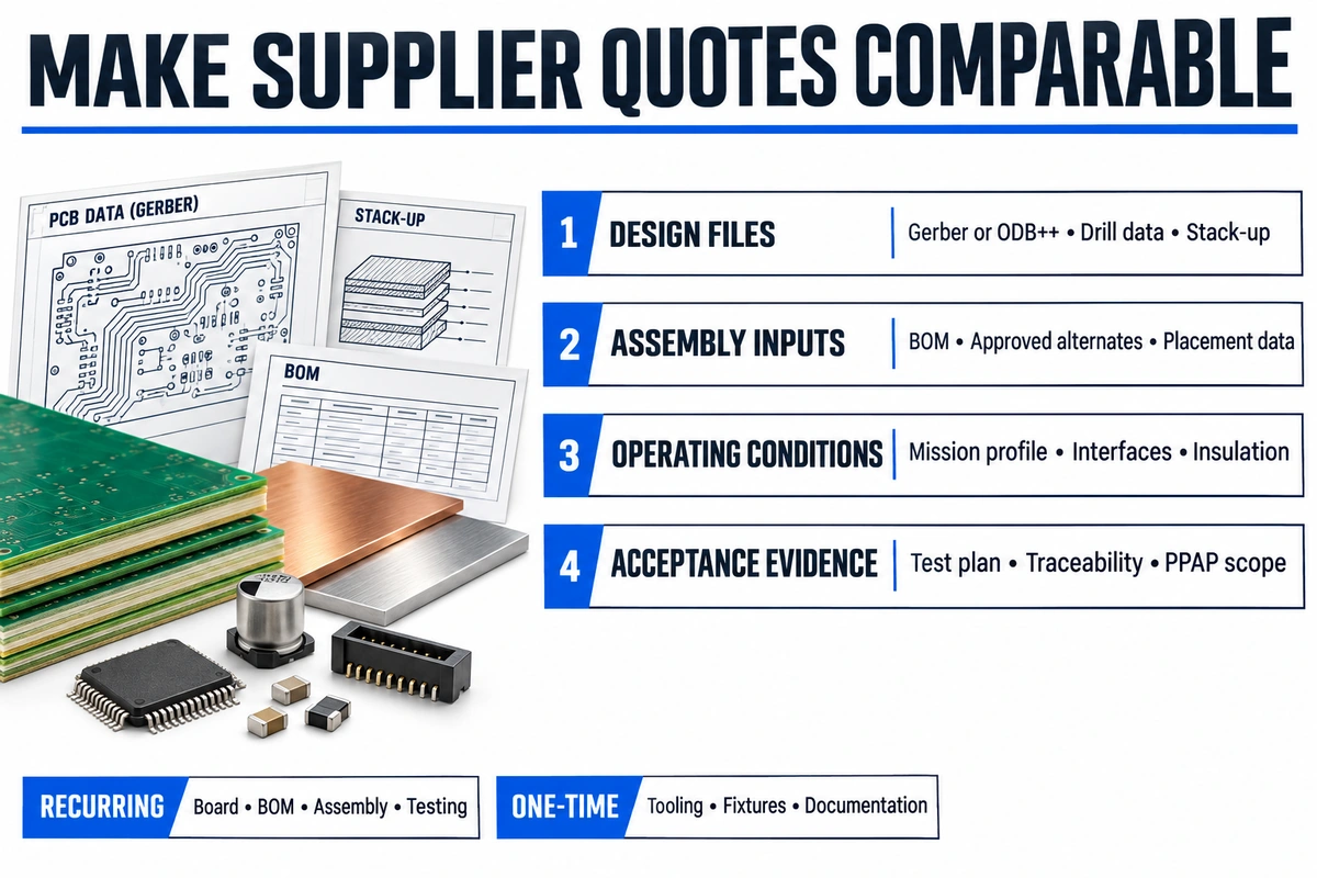
To get accurate, apples-to-apples automotive PCB and PCBA quotes, submit a complete technical package that locks the stack-up, IPC class, AVL BOM, test coverage, and PPAP scope, while separating recurring unit pricing from NRE and test fixtures.
1. Send the Complete Engineering & Operating Specification Package
- Fabrication Files & Stack-Up Drawing: RS-274X Gerber or ODB++ / IPC-2581 files, NC drill files (with press-fit tolerances flagged), master fabrication drawing specifying IPC-6012F + IPC-6012FA Class 3 (or Class 2), laminate slash sheet (e.g., IPC-4101/126 + CTI group), copper weights, surface finish, solder mask type, and panel array drawing.
- Controlled-Impedance & RF Table: Target impedances (50 Ω RF, 100 Ω Ethernet, 120 Ω CAN or transceiver-specific target), tolerances, reference layers, and exact RF laminate callouts (e.g., Rogers RO3003 / RO3003G2) marked “No Substitution Without Written Engineering Approval.”
- BOM & Assembly Data: Pick-and-place centroid file, assembly drawing, and structured BOM listing full Manufacturer Part Numbers (MPNs), AEC-Q100/Q101/Q200 grades, moisture sensitivity levels, and approved AVL alternates.
- Inspection, Test & Cleanliness Protocol: Required bare-board E-test, TDR coupons, solder-float microsections, 3D SPI/AOI/AXI void criteria, ICT coverage, functional test (FCT) procedure/firmware, cleanliness validation (SIR / Ion Chromatography qualification + ROSE monitoring), and conformal coating map.
- Quality, Traceability & PPAP Scope: Required PPAP level (e.g., Level 3), IMDS / RoHS / REACH reporting, 2D DataMatrix format, record retention period (typically 10–15 years), and prototype/pre-series/annual volume schedules.
2. Verify Manufacturing Site Scope and Sample Deliverables
Audit the physical factories performing bare-board fabrication and SMT assembly, verify active quality certificates (ISO 9001, IATF 16949), confirm UL 94V-0 flammability recognition for the specified laminate and board thickness per UL combustion standards, and review a real sample microsection report, TDR log, and Control Plan before awarding the program. When starting an automotive PCB assembly discussion, clarify upfront which steps are handled in-house versus through qualified partners, and align the quality documentation package to your program stage.
3. Itemize Recurring Unit Price vs. NRE, Tooling, Testing, and PPAP Costs
Require suppliers to break quotes into Recurring Unit Price (bare PCB, BOM, SMT/THT labor, inline test cycle time) and Non-Recurring Engineering (NRE) (CAM tooling, laser stencils, selective-solder pallets, ICT/FCT fixtures, microsection/cleanliness lab reports, and PPAP documentation). A quote that looks significantly cheaper on unit price often omits 3D AXI X-ray, IPC-6012 Class 3 plating, conformal coating masking fixtures, or PPAP deliverables—shifting hidden engineering risk back onto your team.
8. Frequently Asked Questions
Can FR-4 Be Used for Automotive PCBs?
Yes—high-Tg FR-4 (IPC-4101/126 or /129) is the primary substrate for the majority of automotive ECUs, including body controllers, instrument clusters, BMS control boards, and under-hood modules up to +125°C. Mid-Tg FR-4 (Tg ≥ 150°C) often suffices for climate-controlled cabin electronics, whereas under-hood and lead-free multilayer builds should specify Tg ≥ 170°C, Td ≥ 340°C and low Z-axis expansion (≤ 3.0%). Only high-heat-flux power stages (requiring IMS or ceramic substrates) and 76–81 GHz radar antennas (requiring PTFE/hydrocarbon RF laminates) must move beyond FR-4.
Do All Automotive PCBs Need IPC Class 3?
No—IPC Class 3 is standard for safety-critical (ASIL B–D), powertrain, braking, steering, and high-thermal-stress under-hood/ADAS modules, but it is not mandatory for every board in a vehicle. Non-safety cabin infotainment or comfort modules frequently use IPC-6012 Class 2 or Class 2 with selected Class 3 attributes—most commonly specifying Class 3 ≥ 25 µm through-hole copper plating for thermal-cycling durability while keeping Class 2 external feature tolerances to optimize yield. Always state the exact class, revision (IPC-6012F), and automotive addendum (IPC-6012FA) on your master drawing.
Can AEC-Qualified Components Replace Board-Level Validation?
No—AEC-Q100, AEC-Q101, and AEC-Q200 qualify the individual component, not the populated PCBA. Once reflowed onto a PCB, CTE mismatch between the component package (3–8 ppm/°C) and the laminate (14–17 ppm/°C in X/Y) stresses the solder joints. You must still validate the assembled board using AEC-Q007, IPC-9701 thermal cycling, and ISO 16750 climatic, transient, and vibration tests.
What Temperature Range Should an Automotive PCB Meet?
Match the temperature rating to the vehicle mounting zone per OEM environmental specs and AEC-Q100 reference grades: -40°C to +85°C for passenger cabins (Grade 3), -40°C to +105°C for cabin hot zones and chassis modules (Grade 2), -40°C to +125°C for under-hood ECUs (Grade 1), and -40°C to +150°C for on-engine and transmission mechatronics (Grade 0). Always add internal I²R self-heating (ΔT) to the maximum ambient temperature and keep peak board temperature at least 20°C to 30°C below the laminate’s Tg.
What Drives Automotive PCB Manufacturing Cost?
Six main factors drive automotive PCB and PCBA cost:
- Substrate Material: Upgrading from high-Tg FR-4 to high-CTI (≥ 600 V) laminates, hybrid 77 GHz PTFE stack-ups (such as Rogers RO3003/RO3003G2), or Si3N4/AlN ceramic substrates.
- Interconnect Complexity: Sequential lamination, laser microvias (1+N+1 or 2+N+2 HDI), back-drilling, or resin-plugged and capped vias (IPC-4761 Type VII).
- Copper Weight & Plating Class: Heavy copper (3 oz–10 oz) and IPC-6012 Class 3 (≥ 25 µm hole-wall copper + 0° breakout), which tighten annular rings and plating residence times.
- AVL Component Sourcing: Specifying AEC-Q100 Grade 0/1 ICs and AEC-Q200 soft-termination passives with lot traceability.
- Inline & Lot Testing: Adding 100% 3D AXI X-ray, bed-of-nails ICT, custom FCT rigs, selective conformal coating, and solder-float microsections.
- NRE & PPAP Documentation: One-time tooling, test fixtures, SIR/cleanliness lab validation, and PPAP Level 3 packages.
When Does a Component or Material Change Require Requalification?
Any post-PPAP change to laminate brand/slash sheet, copper weight, solder mask, solder alloy, component MPN/wafer fab/assembly site, reflow profile, or manufacturing location requires formal Process Change Notification (PCN) and customer review before implementation. Under AIAG PPAP (4th Edition) and AEC-Q100 Rev J Table 3, engineering and quality teams assess the affected failure modes via FMEA to determine whether delta-qualification testing and a revised Part Submission Warrant (PSW) are required.
About This Guide
This technical guide is compiled from public specifications, test methods, and engineering application notes from IPC (Global Electronics Association), the Automotive Electronics Council (AEC), ISO, IEC, UNECE, IATF, AIAG, UL, Texas Instruments, Rogers Corporation, Monolithic Power Systems, Analog Devices, and Infineon as of November 2026. It is designed to help hardware engineers, quality evaluators, and sourcing managers translate vehicle mission profiles into actionable PCB specifications and comparable supplier RFQs. Always govern final part acceptance through the contractually invoked standard revisions, OEM customer-specific requirements (CSRs), and approved DVP&R / PPAP validation plan.
References & Sources
- IPC Standards Revision Table (IPC-6012F, IPC-6012FA, J-STD-001J/JA, IPC-A-610J/JA, IPC-WP-023) — Global Electronics Association
- AEC Component Qualification Documents Directory (AEC-Q100, Q101, Q200, Q007) — Automotive Electronics Council
- ISO 16750-1:2023 Road Vehicles — Environmental Conditions and Testing for Electrical and Electronic Equipment — ISO
- CISPR 25:2021 Vehicles, Boats and Internal Combustion Engines — Radio Disturbance Characteristics — IEC
- About IATF & IATF 16949 Quality Management System — International Automotive Task Force
- Production Part Approval Process (PPAP), Fourth Edition — AIAG
OrinewPCB
Discuss Your Automotive PCB Fabrication and Assembly Scope
Ready to move your automotive board from layout review to prototype or serial production? Share your Gerber/ODB++ files, stack-up drawing, BOM, target quantities, and inspection/testing requirements (IPC-6012 Class 2/3, TDR impedance, 3D AXI X-ray, ICT/FCT, or custom quality documentation) with OrinewPCB to receive an itemized engineering DFM review and quotation.
- +PCB Fabrication
- +Turnkey PCB Assembly
- +DFM & Testing Support
Related Articles
- PCB DFM Checklist — Verify annular rings, drill-to-copper clearances, solder mask dams, and panelization before releasing files to fabrication.
- PCBA Conformal Coating Guide — Compare acrylic, silicone, and urethane protective coatings (25–75 µm), masking rules, and inspection controls.
Get Quote Free